
The DARPA Microsystems Technology Office is developing revolutionary materials, devices and integration techniques for meeting the performance requirements for advanced microwave and RF systems. The DARPA Compound Semiconductor Materials on Silicon (COSMOS) program focused on the development of new methods to tightly integrate compound semiconductor (CS) technologies within state-of-the-art silicon CMOS circuits in order to achieve unprecedented circuit performance levels. The DARPA Diverse Accessible Heterogeneous Integration (DAHI) program is continuing that work by developing heterogeneous integration processes to intimately combine advanced CS devices, as well as other emerging materials and devices, with high-density silicon CMOS technology. Taken together, these programs are addressing many of the critical challenges for next-generation microwave and RF modules and seek to revolutionize DoD capabilities in this area.
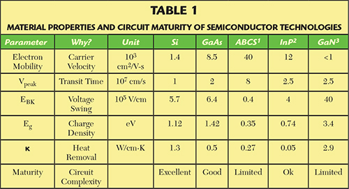
Notes: 1) ABCS-antimonide-based CS, InAs channel, 2) InGaAs channel, 3) SiC substrate
Modern microwave and RF systems are under constant pressure to make use of the spectrum in sophisticated ways, while working within limited power budgets on platforms with reduced size and weight. The compound semiconductor electronics industry is well-positioned to address these challenges, due to the superior properties and diversity of CS materials. For example, high electron mobility and peak velocity of InP-based material systems have resulted in transistors with fmax above 1 THz1 as well as ultra-high-speed mixed-signal circuits.2 The wide energy bandgap of GaN has enabled large voltage swings as well as high breakdown voltage RF power devices.3 Excellent thermal conductivity of SiC also makes tens-of-kilowatt power switches possible.4 Additionally, on-chip high Q micro-electromechanical resonators and switches in various materials, such as AlN, have been demonstrated that potentially can be used for clock references and frequency selective filters.5
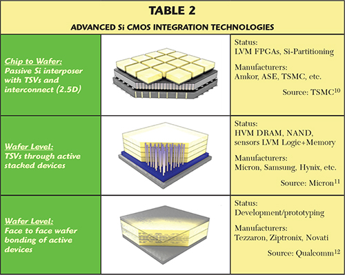
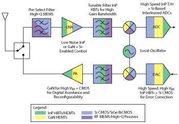
Figure 1 A representative transceiver system is a typical application that can leverage heterogeneous integration.
As indicated by Table 1, compound semiconductors exhibit many superior properties relative to silicon technology. On the other hand, silicon CMOS-based digital technologies have achieved tremendous levels of complexity and integration, while also demonstrating high levels of yield and manufacturability. At the same time, RF CMOS6 and SiGe HBT7 device speeds have continued to increase into the multi-100 GHz regime, albeit at the expense of breakdown voltage. These facts can be attributed to the aggressive device scaling and the advanced levels of back-end-of-line integration driven by Moore’s Law over the past 50 years. In addition, Si-based digital correction and linearization techniques8 have become critical to achieve excellent RF and mixed-signal circuit performance despite drawbacks of the material system.
Given these trends, it is our view that the future of CS electronics depends not on displacing Si, but rather on heterogeneous integration of compound semiconductors with silicon technology in a way that will allow the advantages of the two technology types to be optimally combined. In particular, heterogeneous integration enables size reduction that is critical for miniaturized arrays that are required for 5G proliferation.9
The semiconductor industry has approached the challenges of heterogeneous integration primarily at the macro-scale with assembly-based approaches, such as package and IC stacking with wire bond or flip-chip interconnects. This facilitates pre-integration testing of components, as well as flexibility in selection of device technology and suppliers. More advanced technologies based on interposers and wafer-level assembly are currently gaining traction (see Table 2), but these are primarily for homogeneous integration of Si devices (e.g., logic and memory, FPGAs) and reflect a range of maturity levels.
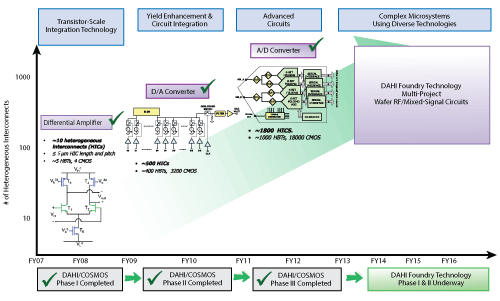
Figure 2 Timeline of DARPA investment in heterogeneous integration for microwave applications.
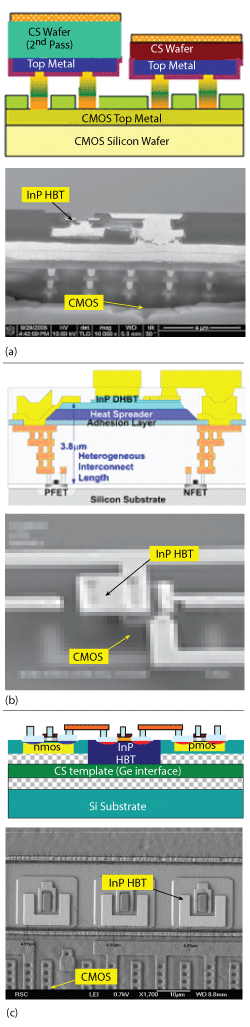
Figure 3 Heterogeneous integration processes being pursued in the DAHI/COSMOS thrust: micrometer scale assembly (a) epitaxial layer printing (b) and monolithic epitaxial growth using a multi-layered lattice-engineered substrate (c).
Figure 1 illustrates the potential impact of heterogeneous integration in RF/mixed signal systems, using a representative transceiver as an example. Essentially all major components in a typical transceiver can benefit from the reduced parasitics of heterogeneous integration, utilizing the benefits of high-performance CS materials with the control and calibration capabilities of Si CMOS.
In order to realize the value of heterogeneous integration for DoD microwave systems, DARPA has invested in heterogeneous integration of microwave technology through several programs. A timeline overview of these programs is shown in Figure 2.
DARPA COSMOS Program
The DARPA Compound Semiconductor Materials on Silicon (COSMOS) program, initiated in 2007, focused on the development of new methods to tightly integrate CS technologies within state-of-the-art silicon CMOS circuits, in order to achieve unprecedented circuit performance levels. COSMOS explored three different approaches (see Figure 3) to achieving InP BiCMOS integrated circuit technology, featuring InP HBTs and deep submicron Si CMOS13, 14, 15 for RF and mixed-signal applications. These approaches included micrometer-scale assembly of InP chiplets with Si CMOS after completion of back-end-of-line (BEOL) processing,13 an epitaxial layer printing approach14 in which unprocessed InP-based heterostructures are transferred to a fully processed Si CMOS substrate and a monolithic “middle-end-of-line” approach15 in which InP HBTs are heteroepitaxially grown coplanar with Si CMOS using a multi-layered Si-based substrate platform.16
These three approaches all achieved success demonstrating heterogeneously integrated differential amplifier circuits using InP HBTs as the differential pair and Si CMOS for the load and current source transistors, resulting in world-record DC gain-unity gain-bandwidth products. In later stages of the COSMOS program, performers demonstrated more complex heterogeneously integrated mixed-signal circuit designs, including digital-to-analog converters (DAC) and analog-to-digital converters (ADC). These circuits are utilizing a number of advanced calibration and self-healing techniques that are enabled by the heterogeneous integration of deep submicron Si CMOS with high speed InP HBTs. Due to the required circuit complexity, these calibration and self-healing techniques would not be possible in circuits implemented in a purely InP-based technology. However, the InP HBTs provide higher speed, higher breakdown voltage and intrinsically better transistor matching than could be accomplished with a purely CMOS-based mixed signal circuit.
One of the advanced circuits demonstrated in the COSMOS program is an ADC with revolutionary mixed-signal performance in InP BiCMOS technology.17 The ADC design employs a time-interleaved architecture utilizing InP HBTs for track-and-hold circuitry and 130 nm Si CMOS to provide the sub-ADCs and the circuitry required for complex time-interleaving. This ADC represents the most complex heterogeneously integrated circuit to date, with ~1000 InP HBTs, ~16,000 Si HBTs and 2500 Si MOSFETs, with more than 1800 heterogeneous interconnects between the InP HBT chiplet and the Si base chip (see Figure 4). This approach has resulted in an ultra-wideband ADC with state-of-the-art signal-to-noise-and-distortion (SINAD) ratio of over 30 dB across frequency ranges of 2.75 to 8.75 GHz and 14.25 to 20.25 GHz (see Figure 5). The COSMOS ADC performs on par with 32 nm ADCs18 despite using 130 nm CMOS, demonstrating the power of heterogeneous integration to improve the performance of older Si CMOS or augment advanced Si CMOS as the integration process is compatible across nodes.
In another COSMOS project, a team of performers at Raytheon/MIT has demonstrated a process for the monolithic integration of GaN HEMTs and Si CMOS on a modified silicon-on-insulator (SOI) wafer. The SOI wafer consists of a Si (111) handle substrate and Si (100) device layer. By opening windows through the Si device layer and buried oxide layers, GaN HEMT structures can be epitaxially grown in the windows on the Si (111) surface, as shown in Figure 6a. Using this approach, the Raytheon/MIT performers demonstrated the world’s first monolithically integrated GaN and CMOS RF amplifier circuit (see Figures 6b and 7) using heterogeneously interconnected GaN HEMTs and pMOS gate bias control.19
COSMOS Multi-Project Wafer
During the course of COSMOS, an InP BiCMOS multi-project wafer (MPW) activity was also initiated based on the HRL Laboratories DAHI/COSMOS technology using 90 nm CMOS and 0.25 µm InP HBTs. In this effort, InP BiCMOS technology was utilized by nine external circuit design teams.
A team at the University of California, San Diego recently demonstrated a 30 GSPS track-and-hold amplifier on the InP BiCMOS platform.20 Differential output spectra with 1 and 31 GHz inputs are shown in Figure 8. This InP track-and-hold (T/H) amplifier on an InP BiCMOS platform represents a key building block for interleaved ADCs, enabling complex interleaving using advanced Si CMOS for high bandwidth, high resolution performance.
An additional circuit design fabricated through the DAHI/COSMOS MPW effort is a four-stage W-Band low-noise amplifier (LNA), designed by a team from the Air Force Research Laboratory.21 Measured results indicate a noise figure (NF) as low as 5.7 dB at 92 GHz (NF < 7.2 dB from 75 to 100 GHz), peak gain of 27.7 dB (gain > 20 dB from 75 to 100 GHz) and power dissipation of 19.2 mW from 75 to 100 GHz. Plots of gain and noise figure versus frequency are shown in Figure 9. This device demonstrated superior noise figure, gain-bandwidth product and power dissipation compared to SiGe BiCMOS W-Band LNAs.
Diverse Accessible Heterogeneous Integration (DAHI)
The COSMOS program significantly expanded the state of the art in heterogeneous integration technology and demonstrated the potential of this technology for producing revolutionary microsystem capabilities. In order to build upon this success, a new DAHI Foundry Technology thrust was initiated22 in 2013 to advance the diversity of heterogeneous device and materials available in a silicon-based platform and make this technology available to the greater DoD and commercial microsystems design community through an accessible, manufacturable foundry for device-level heterogeneous integration. This foundry includes a wider array of materials and devices (including, for example, multiple electronics and MEMS technologies) with complex silicon-enabled (e.g., CMOS) architectures on a common silicon substrate platform. The goal of the DAHI Foundry Technology thrust is to develop a mature, reliable heterogeneous integration technology and to establish cost-effective access to sustainable DAHI foundry capabilities that will enable microsystem designers to choose a range of available semiconductor technologies for transistors or circuit building blocks, to optimize performance of novel advanced microsystems. This capability will not only have significant impact on the performance of both military and commercial microsystems, but it also represents a new paradigm for the CS electronics community.
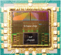
Figure 4 Micrograph of COSMOS ADC showing InP chiplet and Si CMOS base chip.
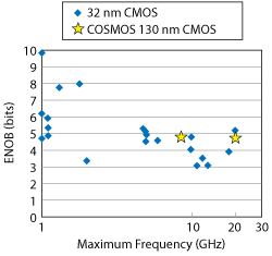
Figure 5 Effective number of bits (ENOB) vs. maximum frequency for state-of-the-art ADCs compared to the COSMOS ADC. COSMOS performs on par with 32 nm ADCs despite using 130 nm CMOS.
In order to realize this goal of highly flexible, diverse heterogeneous integration, an assembly-based multi-technology integration process was developed. This approach confers a number of important advantages for the establishment of a diverse, accessible foundry technology. By conducting the heterogeneous integration after standard BEOL processing, no process changes are required for the Si base or CS technologies being integrated. This allows rapid introduction of new process technologies within the foundry. Other approaches, in which heterogeneous integration occurs prior to or during BEOL processing, require significant levels of process change with often extensive process development timescales and budgets. Only a post-BEOL heterogeneous integration approach can allow rapid integration of third-party technologies into a foundry. This allows the foundry to easily incorporate advances in Si and CS technology nodes into their technology offerings.
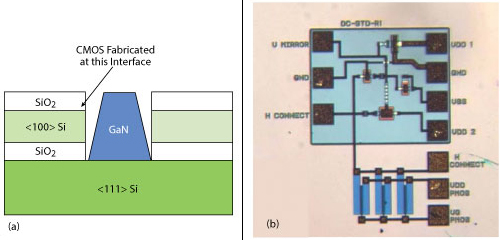
Figure 6 Cross-sectional schematic of GaN growth on multi-layered Si-based substrate (a). Optical micrograph of Raytheon/MIT’s monolithic heterogeneously integrated GaN HEMT + CMOS RF power amplifier circuit (b).
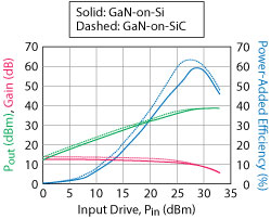
Figure 7 Representative microwave measurements at 10 GHz for the GaN HEMTs shown in Fig. 6 (solid lines) compared to control samples fabricated on SiC substrates (dashed lines).
Recently, a DAHI multi-project wafer run was demonstrated23 utilizing 0.25 µm InP HBTs and 0.2 µm GaN HEMTs heterogeneously integrated with 65 nm Si CMOS (see Figures 10 and 11). This is the first known instance of heterogeneous integration of three device technologies at the transistor level. This heterogeneous integration process utilizes a chiplet assembly-based approach occurring after the completion of BEOL processing. This allows maximum flexibility for the inclusion of novel technologies and requires no changes to the technologies to be integrated. Initial characterization of process control monitors indicates high yield of heterogeneous interconnects among all technologies; characterization is still underway. This multi-project wafer included numerous designs which yielded, including a heterogeneous integrated Q-Band VCO-amplifier chain.24 The InP VCO demonstrated 2 GHz of tuning range at 35 GHz while the GaN amplifier provided 15 dB gain. Output power versus frequency for the VCO-amplifier chain is shown in Figure 12. Other circuits from the multi-project wafer run are currently being tested.
IP Reuse in Heterogeneous Integration
Advances in heterogeneous integration have enabled groundbreaking system performance, but proliferation of the technology will depend on the development of robust and efficient design methodologies. Looking ahead, this challenge is further complicated by the dramatic increase in the complexity and performance requirements of electronic systems. For instance, while early mobile phones could only handle one low bandwidth RF signal, today’s mobile devices are packed with technology that enables Wi-Fi, Bluetooth, near field communications (NFC), AM/FM, Qi and GPS in addition to multiple cellular bands. In the digital domain, field programmable gate arrays (FPGAs) have enabled designers to greatly reduce design time and increase system longevity by providing in-field programmability. However, microwave and mixed signal technologies lack a well-developed field-programmable integrated circuit capability. Consequently, increasingly complex custom application-specific integrated circuits (ASICs) need to be developed to meet the needs of modern microwave systems. Since design costs have become the largest fraction of chip development for low-volume producers like the DoD, constantly designing customized solutions is becoming prohibitively expensive and forcing many designers to compromise performance and capability for cost and design time.
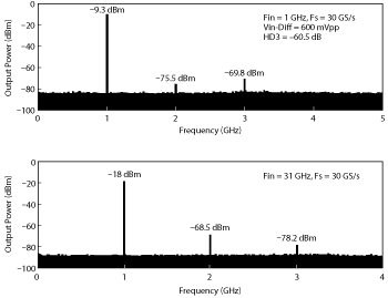
Figure 8 Differential output spectra for InP BiCMOS T/H amplifier20 (used with permission).
The superior performance of advanced CS device technology offers a path towards meeting future microwave system requirements, but the lack of accessible and cost-effective integration strategies limits their use. By expanding upon recent demonstrations of device-level heterogeneous integration with a circuit design block intellectual property (IP) reuse strategy, designers could leverage IP blocks developed across the DoD and commercial markets to choose technologies that best accomplish a mission, rather than being constrained to a single technology or process node. Such design blocks can be implemented as standardized chiplets, which can be assembled on a standardized interposer substrate to create high-performance microwave systems for a wide variety of defense system needs. Implemented correctly, this new design flow will drastically reduce design cost and development time, while enhancing system flexibility. This vision is depicted in Figure 13.
There are many challenges faced in successfully implementing this vision, such as the creation of an IP reuse ecosystem that can manage IP blocks from various process modules (e.g., Si, GaAs, GaN, InP and SiGe) across the design and fabrication cycle. Additionally, developing a design flow that properly handles device modeling, documentation and easy integration with commercial design tools will need to be addressed. Finally, expansion of the heterogeneous integration strategy demonstrated in DAHI to the wider design community to enable any current or future process module to be combined interchangeably using standard interfaces is needed to unlock the full potential.
The benefit of an ecosystem that enables rapid deployment of heterogeneous IP would be immense. Future designs could be optimized to fully leverage the advantages of the wide range of available technologies. More importantly, reusing IP blocks would reduce design cycle times and greatly lower design costs. DARPA sees development of IP reuse methodologies as a priority for further progress in heterogeneous integration.
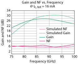
Figure 9 Gain and noise figure versus frequency for InP BiCMOS W-Band LNA21 (used with permission).
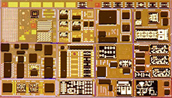
Figure 10 Micrograph of DAHI multi-project wafer fabricated reticle23 (used with permission).
Acknowledgments
The authors would like to thank the program participants in the DARPA COSMOS, COSMOS MPW and DAHI Foundry Technology programs. The authors also thank the COSMOS, COSMOS MPW and DAHI government team members for their support. Finally, the authors thank the original DARPA program managers: Sanjay Raman (DAHI) and Mark Rosker (COSMOS).
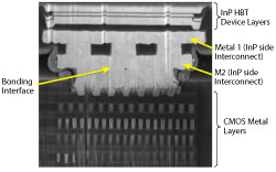
Figure 11 SEM FIB cross section of DAHI Foundry Technology heterogeneous interconnect (HIC)23 (used with permission).
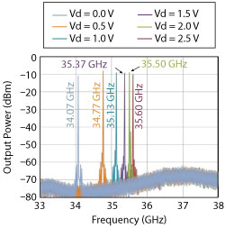
Figure 12 Heterogeneously integrated VCO-amplifier chain output for various input tuning voltages24 (used with permission).
The views, opinions and/or findings contained in this article are those of the author and should not be interpreted as representing the official views or policies, either expressed or implied, of the Defense Advanced Research Projects Agency.
References
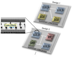
Figure 13 Vision for IP reuse using assembly-based heterogeneous integration.
- R. Lai, et al., “Fabrication of InP HEMT Devices with Extremely High Fmax,” 2008 International Conference on InP and Related Materials, Versailles, France.
- S.E. Turner, D.E. Kotecki, “Direct Digital Synthesizer With Sine-Weighted DAC at 32-GHz Clock Frequency in InP DHBT Technology,” IEEE J. Solid-State Circuits, Vol. 41, No. 10, 2006, pp. 2284-90.
- Y.F. Wu; M. Moore, A. Saxler, T. Wisler and P. Parikh, “40W/mm Double Field Plated GaN HEMTs,” 64th Device Research Conference, 2006, pp. 151-152.
- Cree’s SiC Schottky Diode Chip CPW2-1200-S050B.
- E.R. Crespin, et al., “Fully Integrated Switchable Filter Banks,” IEEE MTT-S, pp.1-3, June, 2012.
- C.H. Jan, et al., “A 45 nm Low Power System-On-Chip Technology with Dual Gate (Logic and I/O) High-k/Metal Gate Strained Silicon Transistors,” IEDM Tech. Digest, pp. 637-640, 2008.
- P. Chevalier, et al., “Towards THz SiGe HBTs,” 2011 IEEE Bipolar/BiCMOS Circuits and Technology Meeting (BCTM), pp. 57-65, 2011.
- Adrian Tang, et al., “A Low Overhead Self-Healing Embedded System for Ensuring High Performance Yield and Long-Term Sustainability of a 60 GHz 4 Gbps Radio-on-a-Chip”, IEEE International Solid-State Circuits Conference (ISSCC), February 2012.
- J. Lipsky, “5G Researchers Seek Spectrum,” EE Times, March 4, 2015.
- F. Lee, “3DICs: Overcoming the Barriers in Designing DCs in a New Dimension,” 2013 Design for 3D Silicon Integration Workshop,” Grenoble, France.
- www.micron.com/products/hybrid-memory-cube/
- K. Arabi, “3D VLSI: Next Generation 3D Integration Technology,” 2015 International Symposium on Physical Design (Keynote), Monterey, Calif.
- A. Gutierrez-Aitken, et al., “Advanced Heterogeneous Integration of InP HBT and CMOS Si Technologies for High Performance Mixed Signal Applications,” IEEE Microwave Symposium Technical Digest, pp. 1109-1112, 2009.
- J.C. Li, et al., “Heterogeneous Wafer-Scale Integration of 250 nm, 300 GHz InP DHBTs with a 130 nm RF-CMOS Technology,” IEDM Technical Digest, pp. 944-946, 2008.
- T.E. Kazior, et al., “A High Performance Differential Amplifier Through the Direct Monolithic Integration of InP HBTs and Si CMOS on Silicon Substrates,” IEEE Microwave Symposium Technical Digest, pp. 1113-1116, 2009.
- C. L. Dohrman, et al., “Fabrication of Silicon on Lattice-Engineered Substrate (SOLES) as a Platform for Monolithic Integration of Si- and GaAs-Based Devices,” Mater. Sci. Eng. B., Vol. 135, No. 3, pp. 135-137, 2006.
- D. Green, et al., “Materials and Integration Strategies for Modern RF Integrated Circuits,” Proc. Compound Semiconductor IC Symp., pp. 1-4, 2014.
- B. Murmann, ADC Performance Survey 1997-2015, http://web.stanford.edu/~murmann/adcsurvey.html.
- W. E. Hoke, et al., “Monolithic Integration of Silicon CMOS and GaN Transistors in a Current Mirror Circuit,” J. Vac. Sci. Tech. B 30(2), pp. 02B101-1-6, 2012.
- T.D. Gathman, et al., “A 30GS/s Double-Switching Track-and-Hold Amplifier with 19dBm IIP3 in an InP/Si BiCMOS Technology,” Proc. ISSCC, 2014.
- P. Watson, et al., “A Wide-Bandwidth W-Band LNA in InP/Si BiCMOS Technology,” Proc. Intl. Microwave Symp., 2014.
- www.darpa.mil/Our_Work/MTO/Programs/DAHI/DAHI_Foundry_Technology.asp.
- D. Scott, et al., “Diverse Accessible Heterogeneous Integration (DAHI) Foundry Establishment at Northrop Grumman Aerospace Systems (NGAS),” Proc. IPRM, Santa Barbara, 2015 (submitted).
- Y.C. Wu, et al., “InP HBT/GaN HEMT/Si CMOS Heterogeneous Integrated Q-Band VCO-Amplifier Chain,” Proc. IPRM, Santa Barbara, 2015 (submitted).