
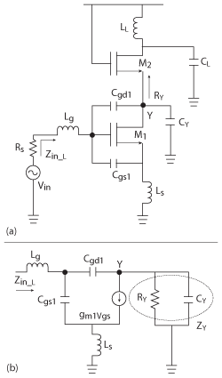
Figure 1 The L-CSLNA (a) and its small signal circuit (b).
A capacitive feedback circuit along with a π-matching network is proposed to achieve the input matching condition without gain trade-off for the common-source low noise amplifier (CSLNA). The π-matching network introduces an additional degree of design freedom and allows the LNA to achieve high gain. Designed for the 2.4 GHz ISM band, the proposed LNA achieves a measured gain of 21.5 dB with an S11 of -12 dB while consuming only 0.6 mW. The NF is 4.9 dB and the IIP3 is -12 dBm.
Nowadays, it is normally desirable to have a high gain LNA in most wireless receivers. Serving as the first active block in the receiver chain, an LNA should provide enough gain to overcome the noise contribution of the subsequent stages and add as little noise as possible. However, in some wireless standards such as the IEEE 802.15.4, the LNA’s noise figure (NF) is not a critical performance parameter.1,2 The NF requirement can be relaxed to allow optimization on other design parameters such as gain, power consumption and chip area. The LNA presented in this article is designed for the IEEE 802.15.4 standard.
Popular LNA topologies are the inductive source-degeneration common-source LNA (L-CSLNA), the common-gate LNA (CGLNA) and the resistive feedback LNA (RFLNA). The L-CSLNA is generally preferred for ultra-low power narrow-band applications due to its ease of input matching, high gain and low noise.3-6 However, its gain performance is limited by the input matching condition. There exists a trade-off between high gain and good input matching in the L-CSLNA.
In this article, an LNA, where the input matching is realized by a capacitive feedback scheme and a π-matching network, is proposed. The capacitive feedback helps to reduce the number of inductors needed for input matching, when compared to the L-CSLNA. Moreover, higher gain and more degrees of design freedom are achieved with the use of the π-matching network. The concept of utilizing capacitive feedback for input matching has been implemented by Chung and Shahroury.7 However, the LNA used has a non-cascode structure. In order to have high reverse isolation, it makes use of a multi-stage structure, which results in very high power consumption. The proposed LNA has a single stage cascode structure. The detailed analysis on input matching, gain and NF are presented. The LNA was implemented using the IBM 0.13 μm Rf CMOS technology.
Inductive Source-degeneration Common-source LNA
The schematic of the L-CSLNA and its equivalent small signal circuit for input impedance analysis are shown in Figure 1. CY includes all parasitic capacitances at node Y and can be approximated as:

RY is the total impedance looking into the source of M2 from node Y. In this circuit, RY can be approximated to be 1/gm2 where gm2 is the transconductance of transistor M2. The L-CSLNA’s input impedance is derived to be:
where ω is the operating frequency, Cgs1 and Cgd1 are the parasitic gate-source and gate-drain capacitance and gm1 is the transconductance of transistor M1. When Cgd1 → 0, Zin_L can be simplified to:
which is consistent with the classical result. At the resonant frequency, the input impedance, Rin_L, equals to gm1Ls/Cgs1 and the transistor’s transconductance, gm1, is effectively boosted to Geff_Lgm1 where Geff_L is:
and ω0 is the resonance frequency. The noise factor of this LNA at the input matching condition is:
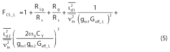
In Equation 5, RLg is the parasitic series resistance of inductor Lg, Rg is the gate resistance of transistor M1,  and
and  are the drain current noise of transistor M1 and M2, respectively, and
  is the input source voltage noise. A large gm1 and small Cgs1 are desired to achieve high gain and low noise.4,5 Due to the input matching condition, the value of Ls is normally quite small. The requirement of small Ls sometimes becomes a nuisance for the LNA design, because not all the inductor values are available in the Process Design Kit (PDK).
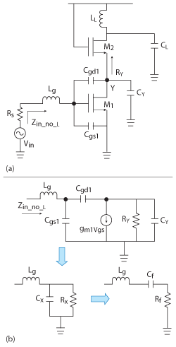
Figure 2 The L-CSLNA (a) and its equivalent small signal (b).
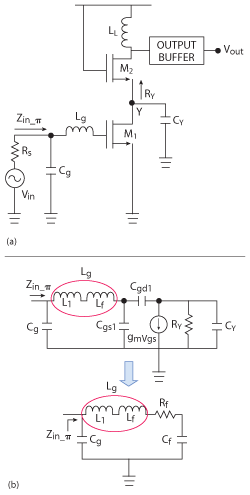
Figure 3 The proposed LNA (a) and its equivalent small signal circuit (b).
The Proposed Capacitive Feedback CSLNA with P-matching Network
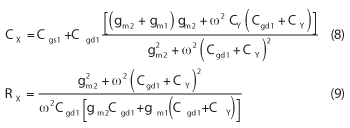
The LNA introduced by Cheng7 uses the parasitic gate-drain capacitance of the input device and the output capacitance, CL, to form the capacitive feedback matching network. Only one inductor was used to realize the input matching. However, the analysis is only applicable for the non-cascode structure. For the CS topology, in order to have high reverse isolation and good stability, a cascode structure is preferred. Here, the analysis for the cascode structure is presented. Its schematic is shown in Figure 2. Based on the small signal circuit (b), the input network of the cascode capacitive feedback LNA can be converted to a series RLC matching network including of Lg, Cf and Rf. The value of Cf and Rf can be derived as:
Cx and Rx can be calculated as follows:
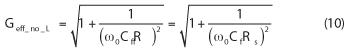
To achieve the input matching, Rf is designed to be equal to Rs. The effective gain of this input matching network is:
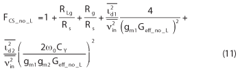
The noise factor at the input matching condition of this LNA can be derived as:
When compared to the L-CSLNA, the capacitive feedback LNA requires a lesser number of inductors for input matching. But this benefit comes with a trade-off of higher NF, which can be observed from Equations 5 and 11. As seen from Equations 4 and 10, the input network’s effective gain of the two LNAs discussed above are limited by the 50 Ω matching condition. To achieve a good input matching, Rf and (gm1Ls/Cgs1) must be matched to 50 Ω. This will restrict the selection of Geff_L and Geff_no_L, therefore limiting the achievable gains of these two LNAs. There exists a trade-off between high gain and good input matching in these two LNAs.
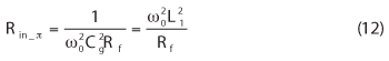
The proposed LNA adds a parallel capacitor, Cg, preceding the gate inductor as seen in Figure 3 to create a π-matching network. It shows the small signal circuit for input impedance calculation of the proposed LNA (b). Rf and Cf are formed by the capacitive feedback mechanism as described above. Inductor Lg can be divided into two smaller parts: L1 and Lf. These two inductors will resonate with Cg and Cf , respectively. The input impedance at the resonance frequency is:
The effective gain of the proposed input matching network is:
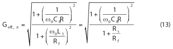
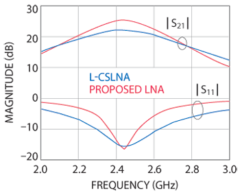
Figure 4 S21 and S11 responses of the proposed LNA and L-CSLNA.
Equation 13 shows that the effective gain of the proposed LNA can be increased by reducing the value of Rf , unlike in the capacitive feedback LNA and the L-CSLNA, where the effective gains are limited by the 50 Ω matching condition. When reducing Rf , the input impedance of the LNA can be matched to 50 Ω by decreasing L1 according to Equation 12. Capacitor Cg and inductor L1 add an additional degree of freedom to the LNA design. The effective gain is no longer limited by the input matching condition. Therefore, the proposed LNA will be able to achieve much higher gain when compared to the L-CSLNA and the capacitive feedback LNA. Figure 4 shows the S21 and S11 responses of the proposed LNA and the L-CSLNA at the same power consumption level and output load condition. The LNAs were designed to have the same input matching at the frequency of interest. The proposed LNA shows a much better gain performance. The gain of the LNA is 3 dB higher than that of the L-CSLNA. The bandwidth (BW) decreases as the effective gain of the matching network is increased. However, as shown, the BW of the LNA in this simulation is still sufficiently large for the required standard.
The noise factor of the proposed LNA is:
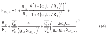
Compared to Equation 11, the noise contribution of RLg has been increased due to the π-network. However, when the LNA is designed such that Geff_π is higher than Geff_no_L, the noise contribution from  can be reduced. Therefore it can compensate for the loss caused by RLg . Moreover, the noise contribution of the cascode stage is also reduced when Geff_π is increased. For a narrow band LNA at frequency f0, the design steps are summarized as follows:
1.) Employ the smallest channel length for the best transistor performance.
2.) To achieve high gain and low noise, the value of Rf is designed to be as small as possible. However, the BW must be kept sufficient for the required application as discussed. In addition, when Rf decreases, the required L1 is reduced, but the required Cg increases. As the negative plate of Cg is connected directly to ground, its value should not be too large.
3.) Derive the value of Cg and L1 from Equation 12.
4.) Determine the value of Lf according to the desired gain and the available chip area. The larger Lf is, the higher the gain gets. Cf resonates with Lf at f0.
5.) Given a specific drain current and the desired Rf and Cf value, design the transistor size and biasing according to Equations 6-9.

Figure 5 Micrograph of the proposed LNA chip.
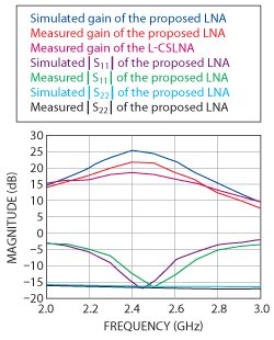
Figure 6 Simulated and measured voltage gain, S11 and S22.
To verify the theory, an LNA was designed and fabricated using the IBM 0.13 μm Rf CMOS technology. Its schematic is shown in Figure 3(a). All inductors are on chip. Inductor LL will resonate with the total capacitance at the drain node of transistor M2 at the frequency of interest. Inductors Lg and capacitor Cg are designed to satisfy the matching condition. The second stage of this LNA is an output buffer. The output buffer was designed to match the output port to the 50 Ω load of the measuring equipment. The loading effect of the buffer is about the same as the mixer loading effect on the LNA stage.
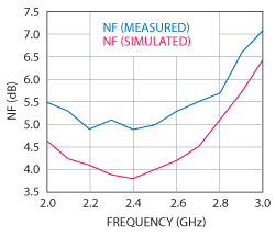
Figure 7 Simulated and measured NF of the proposed LNA.
Measurement Results
A micrograph of the LNA’s chip is shown in Figure 5. The total area including the output buffer and pads is 0.74 × 0.84 mm. Figure 6 shows the voltage gains, S11 and S22, of the proposed LNA. An L-CSLNA, with the same power consumption level and output load condition than the proposed LNA, was also fabricated. The LNA’s voltage gain at 2.4 GHz is 21.5 dB, while the L-CSLNA’s voltage gain is 18.8 dB. The measured gain of the LNA is 2.7 dB higher than that of the L-CSLNA. The proposed LNA has good input and output matching. The S11 value is -12 dB and the S22 value is -16 dB at 2.4 GHz. The corresponding NF is 4.9 dB as shown in Figure 7. The measured NF exceeded the simulated NF by 1 dB. This large difference is attributed to the poor noise modeling and process variation. An IEEE.802.15.4 receiver can tolerate a noise factor of the LNA and the mixer of 11.2 or 10.5 dB.1 This requires a mixer of NF less than 19.8 dB if our LNA is used in the receiver front end. Such a relaxed NF requirement is not difficult to achieve in present CMOS mixer designs. The IIP3 of the LNA is -12 dBm. The core LNA draws 0.6 mA from a 1 V voltage supply. The total power consumption is only 0.6 mW.
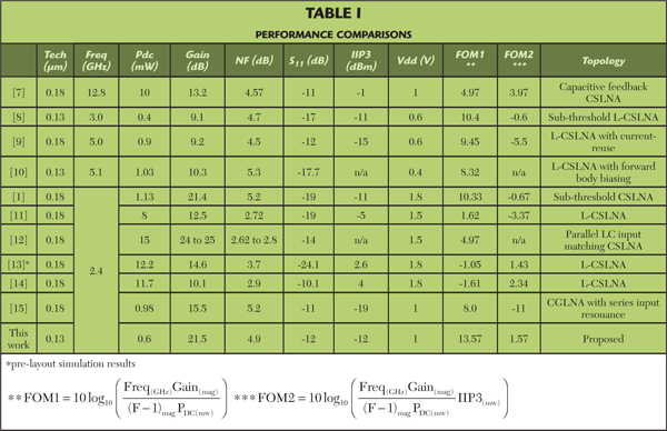
The comparisons of this LNA with results published in the literature are summarized in Table 1. A few LNAs11-14 have better NF but consume much more power than the proposed one. Moreover, such low NF is not necessary for the application,1 and the performance is quite comparable with the proposed one. However, this LNA used a large resistive load to achieve high gain. Therefore, it cannot operate at a low supply voltage such as 1 V. Some of the LNAs13,14 show a trade-off between gain and linearity. Their IIP3 is higher, but the power consumption is much higher and the gain is much lower than the proposed LNA. Based on the FOMs calculated in Table 1, this LNA has the best FOM1 and an acceptable FOM2.
Conclusion
A new input matching topology, without gain trade-off for the CSLNA, was presented. The input network is realized using a capacitive feedback and a π-network. Based on this method, the CSLNA is able to achieve higher gain, while maintaining good input matching and low power consumption. The design method was explained and the LNA was designed and fabricated. The need of source inductor Ls is eliminated and higher gain was achieved when compared to the L-CSLNA. The proposed LNA consumes only 0.6 mW, while providing very high gain, good input matching and moderate NF.
References
- A.V. Do, C.C. Boon, M.A. Do, K.S. Yeo and A. Cabuk, “A Subthreshold Low-Noise-Amplifier Optimized for Ultra-Low-Power Applications in the ISM Band,” IEEE Transactions on Microwave Theory and Techniques, Vol. 56, No. 2, February 2008, pp. 286-292.
- A.V. Do, C.C. Boon, M.A. Do, K.S. Yeo and A. Cabuk, “An Energy Aware CMOS Receiver Front End for Low Power 2.4 GHz Applications,” IEEE Transactions on Circuits and Systems I: Regular Papers, Vol. 57, No. 10, October 2010, pp. 2675-2684.
- A. Meaamar, C.C. Boon, K.S. Yeo and M.A. Do, “A Wideband Low Power Low-Noise Amplifier in CMOS Technology,” IEEE Transactions on Circuits and Systems-I, Vol. 57, No. 4, April 2010, pp. 773-782.
- A. Meaamar, C.C. Boon, M.A. Do and K.S. Yeo, “A 3 to 8 GHz Low-Noise CMOS Amplifier,” IEEE Microwave and Wireless Components Letters, Vol. 19, No. 4, April 2009, pp. 245-247.
- T.H. Lee, The Design of CMOS Radio-Frequency Integrated Circuits,Cambridge University Press, 1998, Cambridge, U.K.
- Y.P. Zhang, K.W. Chew and P.F. Wong, “Analysis and Design of a Fully Integrated CMOS Low-noise Amplifier for Concurrent Dual-band Receivers,” International Journal of Rf and Microwave Computer-Aided Engineering, Vol. 16, No. 5, May 2006, pp. 444-453.
- Y.W. Chung and F.R. Shahroury, “A Low-Voltage CMOS LNA Design Utilizing the Technique of Capacitive Feedback Matching Network,” 2006 IEEE International Conference on Electronics, Circuits and Systems Digest, pp. 78-81.
- H. Lee and S. Mohammadi, “A 3 GHz Sub Threshold CMOS Low Noise Amplifier,” Proceedings of the 2006 Radio Frequency Integrated Circuits (RFIC) Symposium, June 2006.
- H.H. Hsieh and L.H. Lu, “A CMOS 5 GHz Micro-power LNA,” Proceedings of the 2005 Radio Frequency Integrated Circuits (RFIC) Symposium Digest, pp. 31-34.
- D. Wu, R. Huang, W. Wong and Y. Wang, “A 0.4 V Low Noise Amplifier Using Forward Body Bias Technology for 5 GHz Application,” IEEE Microwave and Wireless Components Letters, Vol. 17, No. 7, July 2007, pp. 543-545.
- H.S. Jhon, H. Jung, J. Jeon, M. Koo, B.G. Park, J.D. Lee and H. Shin, “Size Efficient Low-noise Amplifier for 2.4 GHz ISM-band Transceiver,” Microwave and Optical Technology Letters, Vol. 51, No. 10, October 2009, pp. 2304-2308.
- S. Mou, J.G. Ma, K.S. Yeo and M.A. Do, “A Modified Architecture Used for Input Matching in CMOS Low-noise Amplifiers” IEEE Transactions on Circuits and Systems II: Express Briefs, Vol. 52, No. 11, November 2005, pp. 784-788.
- W.C. Cheng, M.G. Jian, K.S. Yeo and M.A. Do, “Design of a Fully Integrated Switchable Transistor CMOS LNA for 2.1 / 2.4 GHz Application,” 2006 European Microwave Integrated Circuits Conference Digest, pp. 133-136.
- L.H. Lu, H.H. Hsieh and Y.S. Wang, “A Compact 2.4/5.2 GHz CMOS Dual-band Low-noise Amplifier,” IEEE Microwave and Wireless Components Letters, Vol. 15, No. 10, October 2005, pp. 685-687.
- T.T.N. Tran, C.C. Boon, M.A. Do and K.S. Yeo, “Ultra-low Power series Input Resonance Differential Common-gate LNA,” IET Electronic Letters, Vol. 47, No. 12, (2011), pp. 703-704.
Thi Thu Nga Tran received her bachelor of engineering degree (Hons.) in electronics from Nanyang Technological University (NTU), Singapore, in 2008. Currently, she is working towards her doctorate in philosophy degree at NTU, Singapore. Her research interests include ultra-low power Rf front-end IC design and mixed-signal circuits for high speed applications.
Chirn Chye Boon received his bachelor of engineering (Hons.) (Elect.) in 2000 and his Ph.D. (Elect. Eng.) in 2004 from Nanyang Technological University (NTU), Singapore. In 2005, he joined NTU as a Research Fellow and became an assistant professor in the same year. Before that, he was with Advanced RFIC, where he worked as a senior engineer. He specializes in the areas of radio frequency & MM-wave circuits and systems design for biomedical and communications applications.
Manh Anh Do received his bachelor of engineering (Hons.) degree and his doctorate in philosophy degree in electrical engineering from the University of Canterbury, Christchurch, New Zealand, in 1973 and 1977, respectively. Between 1977 and 1989, he held various positions, including design engineer, production manager, and research scientist in New Zealand. He was a senior lecturer with the National University of Singapore, Singapore. He joined the School of Electrical and Electronic Engineering, Nanyang Technological University (NTU), Singapore, as a senior lecturer in 1989 and obtained the Associate Professorship in 1996 and Professorship in 2001. Between 1995 and 2005, he was Head of division of circuits and systems, NTU. He was the director of center for integrated circuits and systems from 2007 to 2010. He is currently a member of the NTU Research Council. His current research interests include mobile communications, RFIC design and mixed-signal circuits.
Kiat Seng Yeo received his bachelor of engineering (Hons.) (Elect.) in 1993, and his doctorate in philosophy (Elect. Eng.) in 1996 both from Nanyang Technological University, Singapore. He began his academic career as a lecturer in 1996, and was promoted to assistant professor in 1999 and then to associate professor in 2002. He was Sub-Dean (Student Affairs) from 2001 to 2005. He is a board member of Microelectronics IC Design and Systems Association of Singapore, Member of the Advisory Committee of the Centre for Science Research & Talent Development of Hwa Chong Institution and consultant to statutory boards and multinational corporations in the areas of IC design.