

 As I mentioned in last week’s post, this blog will be a collaborative effort among a number of us with more years of experience in RF test and measurement that we likely want to admit. This week I’d like to introduce Simon Mathias. He is the vice president of sales and marketing for our partner Mesuro Ltd.Simon has spent the over 20 years of his career is the test & measurement industry.
-- Darren McCarthy, Tektronix
One particularly tough RF test challenge is the load-pull characterization of high power devices, such as those used in mobile base-stations. Characterization of these devices at the actual operating power of the final system brings with it a number of challenges.
There are two main approaches for load-pull, either the use of a passive tuner or the use of an active load-pull system. There are challenges for both systems when evaluating a high power device.
For passive systems reaching the very low impedances required to match the DUT can be very difficult as any loss between the tuner and the DUT will reduce the maximum achievable reflection coefficient. In addition stability is a key issue as the out of band impedances for a passive system are uncontrolled and as such can lead to unstable device operation, particularly for large devices.
For an active system the main issue is the required system amplifiers. Some simple math using the low impedance match is required, plus the system loss can easily get us to a requirement for KWs of power to load-pull a 100W device. This problem can be solved through the use of wide-band impedance transformers, which are used to transform the system impedance from the standard 50 Ohms to a more suitable impedance, thus dramatically reducing power requirements.
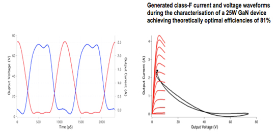
Another approach is rather than directly characterizing the high power device is to scale a unit cell and predict how the device performance scales to higher power. This is often challenging and designers will often find that the performance just does not scale. The reasons are often to do with the device process, with phenomena like knee-walkout and current collapse as well as junction temperature causing significant differences as the device is scaled.
The key then is to identify the cause of the scaling issue. In my opinion the best way to achieve this is through the use of measured voltage and current waveforms. This directly informs the designer of the RF interaction with the device’s DC boundaries. Note that this is problematic particularly for a packaged device as this useful information only exists at the current generator plane. This means that in order to use this approach you must first de-embed the device and package parasitics as shown in the image below.
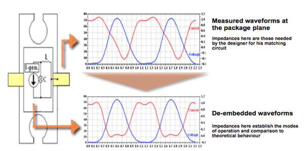
Using the waveforms as shown below, the designer’s ability to understand how a scaled device may perform can be referenced to data on lower power devices and allows the measured data to be more easily used within design simulators prior to final design fabrication.
We‘d like to hear from you. How have you approached this challenge and how do you think the needs of the industry will develop over the next few years? Let’s get the conversation started.