

Microwave circuits are generally susceptible to the effects of copper conductor surface roughness, some less than others. In the last blog, several types of coplanar-waveguide (CPW) circuits were compared to standard microstrip to gauge the effects of copper surface roughness on high-frequency performance. Microstrip circuit performance, in particular, is degraded by high root-mean-square (RMS) values of conductor surface roughness. As circuit designers learned in the last blog, microstrip designs that must minimize loss can benefit from the use of circuit materials with low-profile copper conductors, such as RO4000® LoPro™ series circuit laminates from Rogers Corp. As the last blog pointed out, CPW and conductor-backed CPW (CBCPW) circuits will not benefit at higher frequencies from the use of laminates with low-profile conductors to the same degree as microstrip circuits. But is this also the case with high-frequency or high-speed stripline circuits? Just how does conductor surface roughness influence high-frequency stripline circuit performance?
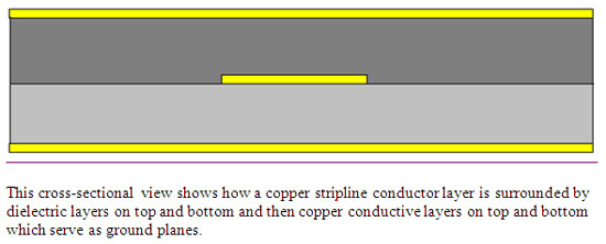
Stripline is a transverse-electromagnetic (TEM) transmission-line medium known for its capability of providing excellent electrical performance as well as its associated challenges in design and manufacturing. Stripline essentially surrounds a conductive signal layer by upper and lower dielectric layers with top and bottom ground planes in a sandwich-like structure. Because of its enclosed structure, stripline is often likened to a “flattened coaxial cable.” Its sealed structure helps minimize radiation losses while also providing good immunity to external noise and isolation from adjacent circuits, but also makes component placement problematic and circuit manufacturing more complex and expensive.
Stripline is not without its signal loss mechanisms, which can lead to greater losses than in microstrip circuits. In microstrip, current flows through the conductor metal but also partially in the surrounding dielectric substrate and partially in the air above the conductive metal and dielectric material. In effect, microstrip has a heterogeneous dielectric composition, with the air above the circuit contributing a relative dielectric constant of approximately 1 and low loss. As frequency increases, current in a microstrip circuit propagates closer to the surface of the conductive metal where, at high enough frequencies, any surface roughness on the metal conductor can influence the signal propagation, increasing conductor loss.
But how does conductor surface roughness affect stripline signal propagation? In stripline, the conductive metal is surrounded by dielectric substrate material. For a given characteristic impedance, such as the 50 Ω common to microwave circuits, stripline circuits typically require a narrower conductor width than a microstrip circuit intended for the same frequency. This narrower conductor width translates into higher conductor loss for stripline than microstrip. Stripline, with its top and bottom ground return paths, will also be affected more by a rough copper conductor surface. Of course, stripline will also benefit more than microstrip from a laminate with a smooth copper conductor surface.
Stripline is used in various configurations for high-speed digital and high-frequency analog circuits, including symmetrical stripline circuits, in which the two ground planes are at an equal distance from the signal trace layer, and asymmetric stripline, where the distances from the signal trace layer to the two ground planes are unequal. In all cases, as signal frequencies/speeds increase, the effects of conductor surface roughness become more pronounced and will have a greater impact on performance.
In stripline as in microstrip, when the signal frequencies increase, and the wavelengths of those signals become small enough to be comparable to the dimensions of the conductor surface roughness, attenuation due to conductor loss will increase as a function of increasing frequency. The amount of loss contributed as a result of the conductor surface roughness can also be impacted by the closeness of the stripline conductor layer to the ground planes—that is, the thickness of a stripline circuit’s dielectric layers can determine the effect that the conductor layer’s surface roughness has on the final loss of the stripline circuit.
The surface roughness of a stripline circuit’s ground planes can also influence conductor losses, especially when those ground planes are closely spaced to the conductor. The surface currents on those ground or reference planes are considerably less than the surface currents on the conductor layer, so surface roughness on those planes will have far less impact on loss than the same surface roughness on the signal plane. Still, a designer should be aware of these loss components when estimating stripline conductor losses.
A stripline construction has a total of four interfaces between copper and dielectric materials, and some of the interfaces can have very different copper surface roughness. The differences are due to how the stripline construction is fabricated.
Stripline can be made in several different ways. One common method is to start with a double-copper-clad laminate, etch the inner layer conductor to form the stripline signal conductor, add prepreg bonding materials as the dielectric layer above the conductor, and then a copper foil above the prepreg to form the top ground plane. With this approach, the copper foil that serves as the top ground plane can have a much different surface roughness than the copper surface roughness of the laminate, which contributes the stripline signal conductor and the bottom ground plane to the stripline construction. Of the four copper-substrate interfaces in this construction, only two of them (signal conductor on dielectric and bottom ground plane on dielectric) are the same, adding to the complexity when developing a model to predict the effects of copper surface roughness.
Another way in which stripline can be fabricated results in three of the four copper-substrate interfaces using the same copper. This approach uses two double-copper-clad laminates which are the same. One is etched on one side to form the signal layer, with the ground plane underneath; the other has one of its copper layers etched away, with the other remaining to form the top ground plane. A thin bonding material layer is used to adhere the material with the signal layer to the bottom of the other laminate that had one side of the copper etched away. Because three of the four copper-substrate interfaces are consistent, modeling and prediction for this stripline construction are much more straightforward.
There can be some benefit in fabricating an “unbalanced” stripline construction which uses a double-copper-clad laminate with rough copper surface, prepreg, and smooth copper on top. As in the first construction approach, the double-copper-clad laminate with rough copper is used for the signal conductor and bottom ground plane. Prepreg is added on top of the signal conductor layer and then a smooth copper foil above the prepreg layer. If the prepreg layer is significantly thinner than the copper-clad laminate, the stripline signal conductor will be closer to the smoother top copper foil. In this stripline construction, two of the copper-substrate interfaces involve the rough copper and two use the smoother copper. The top of the signal plane copper will be smooth as well as the copper foil added above the thin prepreg layers.
Typically, a stripline circuit’s two ground planes are shorted together to prevent the propagation of unwanted modes. This is usually done by forming viaholes parallel and on each side of the signal traces. When developing computer-aided simulations of performance based on stripline technology, it is often useful to apply different conductor roughness profile models as a means of estimating the impact of conductor profile on final circuit performance.
The use of a circuit material with low-profile copper conductor can minimize the stripline conductor loss components that might be caused by a conductor with high RMS surface roughness. It will still suffer some conductor losses, and dielectric losses, and even minimal radiation losses. But by properly understanding the loss mechanisms of a stripline construction, any estimations of loss such as might be performed with a transmission-line calculator such as the MWI-2010 Microwave Impedance Calculator from Rogers Corp. will agree more closely with actual measurements, especially at higher frequencies. And because stripline circuits are susceptible to the losses added by conductor surface roughness effects, stripline designs can be optimized for low-loss performance through the proper application of a circuit material with low-profile copper conductor, such as the RO4000 LoPro laminates from Rogers Corp.
Do you have a design or fabrication question? John Coonrod and Joe Davis are available to help. Log in to the Rogers Technology Support Hub and “Ask an Engineer” today.