
As serial data speeds increase, instrumentation for characterizing and debugging the next generation of protocols is required. A real-time oscilloscope family with 32 GHz of bandwidth and the lowest reported jitter and noise floor has been developed, providing engineers superb signal integrity for characterizing and debugging the fastest interfaces.
The oscilloscope incorporates a new architecture for signal acquisition and a new chipset delivering the performance. It features a new analog frontend chipset developed in an InP HBT process. This process has a number of features allowing for the implementation of broadband circuits operating at very high frequencies. It features several ICs designed in this process: A new preamplifier IC reaching frequencies from DC to 32 GHz, a new sampler IC, a new trigger IC and a new calibration IC.
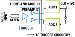
Figure 1 Block diagram of a traditional oscilloscope front-end.
Traditional Architecture
Figure 1 illustrates the traditional architecture used in the previous generation Agilent oscilloscopes. The input signal passes through a variable attenuator, followed directly by a preamplifier IC, responsible for scaling the signal properly, applying offset, and buffering the signal to the analog to digital converters (ADC). To provide enough sample rate to not violate Nyquist, two ADCs sampling at ƒS/2 are interleaved in the architecture described by Figure 1, where ƒS represents the full sample rate of the acquisition channel.
This architecture has several limitations:
- The ADC input bandwidth and sampling aperture must be at least the full RF bandwidth of the oscilloscope
- The preamplifier must drive multiple ADCs (in this case two), with the full RF bandwidth preserved at the interface
- Mismatch associated with the fan-out will manifest as error in the measurement

Figure 2 Sine wave of ƒS/5 inserted into oscilloscope (a). The waveform is then reconstructed from the interleaved samples of ADC 1 and ADC 2 using sin (x)/ x interpolation.
To clarify item 3, a sine wave operating at one-fifth the sample rate is presented in Figure 2. The outputs from the ADCs are interleaved to reconstruct the waveform at full sample rate, shown by the interpolated waveform (b). Sin(x)/x interpolation is used to reconstruct the signal from the sampled data. In this example, ƒS is 40 GS/s and the input waveform is an 8 GHz sine wave. ADC 1 input cannot be seen clearly because it is overlapped by the ADC 2 input waveform. ADC indices in this figure correlate to the ADC indices in Figure 1. By forcing the ADCs to sample 180° out-of-phase, the effective sample rate of the system can be twice that of a single ADC.
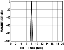
Figure 3 An FFT of the interpolated waveform in Figure 2b.
A Fast Fourier Transform (FFT) of the result in Figure 2 is shown in Figure 3. Note the single tone at ƒS/5, indicating that the waveform is properly reconstructed by the system. Because the preamplifier must drive both ADC blocks, the interface between them is important to match. Mismatch in the interface will cause error in the acquired waveform. As an example, consider the case where the second preamp output channel has less bandwidth than the first output buffer. In this example, 3 dB of loss is added to the second ADC input signal. This is illustrated in Figure 4.
When the samples are interleaved, a new signal is created, which manifests as distortion in the reconstructed waveform, not present in the signal when presented to the oscilloscope input. An FFT of the reconstructed waveform is given Figure 5. The FFT of the interpolated waveform shows a new tone at 12 GHz, not present in the first example, where ADC inputs were well matched.

Figure 4 The ADC 2 input is now attenuated by 3 dB (a). ADC 1 and ADC 2 no longer digitize the same signal. This causes error in the interpolated waveform.
ADC mismatch is another potential source of the error seen in Figure 4. Because two ADCs are used, any mismatch between the two components due to process variation, packaging differences or assembly anomalies will create errors in the user's signal if not addressed properly. To avoid such problems, careful design of the preamplifier/ADC interface is critical. As the frequency capability of the oscilloscope increases, the design becomes more challenging.
As an example, suppose this architecture were used in a system with twice the bandwidth. This requires a sample rate of 2ƒS. Assuming the same ADC converter technology is used, the system now requires four ADCs per acquisition channel, and requires a fan-out of four from the preamplifier module. This fan-out would require twice the bandwidth as the previous generation. With higher input bandwidth also comes more complexity and power in the ADC block itself. Maintaining signal integrity in a system like this is difficult. The new architecture was developed to avoid these issues in high-bandwidth oscilloscopes.
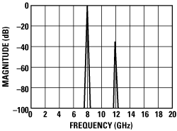
Figure 5 The FFT of the interpolated waveform with ADC input signals mismatched shows a tone at 8 GHz and a new tone at 12 GHz as a result of the mismatch.
The DSO-X Architecture
Figure 6 is a drawing of the new DSO-X architecture. Although very similar to the original architecture, the DSO-X includes a number of new components:
- A full-bandwidth, low-noise preamp, responsible for signal scaling and offset injection
- A high-bandwidth trigger IC
- A new sampler IC, inside the preamp module
As seen in Figure 6, the first ranks of sampling are now contained inside the preamp module, instead of on the CMOS ADC. This is advantageous for a few important reasons. Firstly, the full-bandwidth preamplifier IC now provides only one output to the sampler, instead of fanning-out to multiple ADCs with full channel bandwidth. Because the preamp IC is contained in the same micro-circuit module as the sampler IC, the interface distance is short and does not require long PCB traces, lossy at high frequencies. The RF traces inside the microcircuit can be printed on a low-loss dielectric material, optimizing the interface for high-frequency transmission.
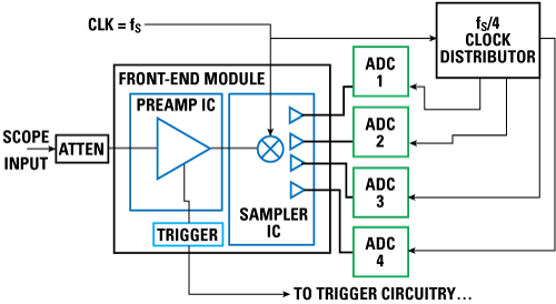
Figure 6 The new DSO-X architecture.
Secondly, because the RF sampling occurs in one IC, mismatch in sampled responses is smaller. In the previous architecture, RF sampling occurred in the ADC technology blocks themselves. Because the ADC samplers exist on separate die, the potential mismatch between the sampling apertures is much greater than the new architecture, where samplers coexist on one die.
Thirdly, because the first ranks of sampling are contained in one proprietary IC, the ADC must no longer accept full-bandwidth to its input. The requirements on the ADC aperture, therefore, are much less, allowing the previous generation of ADC to be used in the new design, and lowering the effective noise bandwidth at the input to the ADC.

Figure 7 The DSO-X front-end module with preamp (A), trigger (B) and sampler IC (C).
The DSO-X Analog Front End
At the heart of the new DSO-X is a new analog front-end module containing three new ICs designed in Agilent's HB2B InP semiconductor process. The module is shown in Figure 7. It contains a new DC to 32 GHz low-noise preamplifier that feeds a 20 GHz trigger IC and a 32 GHz sampler IC. The sampler IC accepts full bandwidth to its input, and drives the four CMOS ADC converters outside of the analog front-end module, after sampling.
The HB2B InP HBT process enables the performance levels achieved. The HBTs available in the process have maximum ƒτ frequencies of 185 GHz at 2 mA/um2 bias current levels. The process incorporates two varieties of thin-film resistor material for low parasitic passive components. Resistive materials available are a 22 ohm/square thin-film material and a 250 ohm/square thin film material. High-density MIM capacitors are also available, with 0.59 fF/um2.

Figure 8 An example of a multi-rank sampling architecture.
Unlike silicon-based HBT processes, the HB2B process has an insulating InP substrate, with a dielectric constant of 12.4. The substrate is 90 um thick. This allows for low parasitic capacitance interconnect and the ability to design spiral inductors with high inductance/length, for input T-coil matching circuits and on-chip filters.
Multi-Rank Sampling
As discussed previously, multiple ranks of sampling are required in the DSO-X architecture to achieve high-bandwidth response. High-frequency sampling is handled by the InP HBT sampling IC in the analog front-end module, while final digitization of the samples is performed in the Agilent CMOS ADC used in previous oscilloscope designs. Figure 8 is an example of how multi-rank sampling can be used to leverage lower-speed ADC technology for a high-bandwidth system.
In this figure, a tranconductance amplifier is used to convert the voltage signal from the preamplifier into a current. This amplifier is responsible for buffering the preamp's output into the first sampler, and must accept full RF bandwidth to its input and drive full RF bandwidth on its output. This output signal, in the form of a current, is fed into an HBT sampling switch labeled "Sampler Cell" in Figure 8. The HBT switch is driven by a sample pulse driver that drives the base of the HBT switch. When the switch is "off", the "VCas" bias voltage shown in Figure 8 is higher than the "clk1" signal, and the RF current is shunted. When the sample pulse fires, the HBT switch conducts current into the output load. The RF current travels through the cascode sample device and is imposed on an impedance to convert the sampled current into a voltage.
The load impedance defines the pulse-shape of the sampled signal, and the first IF bandwidth, once it is converted to a voltage. The IF of the first sampler output requires the previous sample be settled before the peak of the next sample. Therefore, the sampled output of the first IF in Figure 8 must reach its final value in no less than TS, where TS is 1/ƒS, the sampling frequency. While this does not relax bandwidth requirements to the next sampler rank, it does allow for very low jitter sampling and proper response matching. Because all samples pass through a single sampler, all samples are referenced to a single clock. Furthermore, the RF response of the Rank 1 sampler affects all samples in the system, eliminating susceptibility to RF sampler response mismatch, seen previously in Figure 4.

Figure 9 Multi-rank sampler outputs.
The first IF output drives additional transconductance stages. The output of each buffer drives a sampler. These cells sample out of phase, each operating at ƒS/2. Because the sample rate is lower, the IF output of each sampler has more time to settle before the next sample. This is demonstrated in Figure 9. In this figure, the sample pulse output from the Rank 2 sampler can be broader than the original sample stream. The Rank 2 samplers behave as "switches" that route alternating Rank 1 sample outputs to Rank 2 outputs. Because the pulses have more time to settle in the higher ranks of sampling, the bandwidth requirement of the IF is reduced.
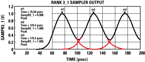
Figure 10 Gaussian IF response of Rank 3.
Finally, the "Rank 3_1" output shown in Figure 9 indicates that Rank 3 output pulses have a longer time to settle than Rank 2 outputs. In the limit, each sample pulse must return to zero just before the next pulse reaches its final value. In Figure 9, the IF bandwidth for each sampler rank has been augmented to make sample location more obvious.
Figure 10 portrays the Gaussian IF response of Rank 3 if the bandwidth is reduced by a factor of 2. The dashed lines in Figure 10 indicate the trajectory of the sample pulses. Note that each pulse settles before the peak of the next pulse in the IF, even with reduced bandwidth.
Figure 11 portrays all sampled outputs from the Rank 3 samplers in Figure 8. The separation of each pulse is exactly 1/ƒS, but because the pulses exist on four separate IF channels, they each have much longer to settle than the Rank 1 sample outputs.
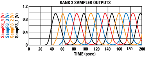
Figure 11 Rank 3 sampler outputs for all Rank 3 samplers shown in Figure 8.
Reduced IF bandwidth is advantageous to the design for several reasons: Lower-power circuits can be used after the sampler, because the bandwidth requirements on circuits following sampling are relaxed; as multiple ranks are used in the sampling process and IF bandwidth requirements are relaxed, driving signals off of the IC using standard PCB traces becomes less challenging than at full RF bandwidths; lower IF bandwidth from the HBT integrated circuit results in lower frequency content to the ADC, reducing susceptibility to high-frequency mismatch, and allowing the architecture to leverage existing CMOS ADC technology.
Many sampling ranks can be used, to the point where IF bandwidth is slow enough for CMOS ADC digitization. Once digitization occurs, the samples must be interleaved properly in time with one another, to reconstruct the waveform at full sample rate, as discussed previously.
Conclusion
As the industry demands high bandwidth measurement capability, it is important test and measurement equipment manufacturers provide solutions for characterizing high-speed signals. The DSO-X achieves high performance levels with a unique sampling architecture, featuring fast HBT-based circuits partnered with CMOS ADC technology. The new architecture provides the industry's lowest reported noise and jitter in the highest bandwidth real-time oscilloscope available.
Acknowledgments
The author would like to thank Kenneth Rush, Dave Dascher, Steve Draving, Mike Lujan, Mike McTigue and Allen Montijo.