
Wire bonding is the most common interconnect method for providing the interconnection between an integrated circuit (IC) and a printed circuit board (PCB), IC-to-IC, or PCB-to-PCB. The two main wire-bonding technologies are ball bonding and wedge bonding. Although ball bonding is faster and much more popular, wedge bonding offers advantages that are well suited for optic-electronic and power devices, where reliability and performance outweighs bonding speed. However, ribbon bonding is a form of wedge bonding where flat ribbon wire is used instead of round wire. Ribbon bonding first came into use in the defense electronics sector, where it was the first interconnection level of choice for GaAs MMICs in millimeter-wave radar. Compared with the round wire, the ribbon wire bonding results in higher reliability because of the larger cross-section at the heel of the bond. There is also less cratering with a ribbon wire because the bond force and ultrasonic are distributed over a larger area.1 In the past few years, several published papers2-4 have compared the mechanical properties for ball and ribbon bonding, but very few papers discussed their electrical performance.
In this article the electrical characteristics of ball and ribbon bonding (round and ribbon wires, shown in Figure 1) were compared, such as wire self-inductance, self-resonant frequency (ƒSR) and insertion loss (IL). In order to objectively compare these parameters, three types of wires were adopted to satisfy the same comparison conditions: 0.5 x 2 mils ribbon wire, 2 mils round wire and 0.8 mils round wire. These wires, made of the same material (gold), loop height and wirelength, were measured up to 20 GHz, to obtain their electrical properties for further comparison.

Figure 1 Two types of wire bonding technologies: (a) ribbon bonding and (b) ball bonding.
Test Method
To carry out the high-frequency measurements for round and ribbon wires, all wires were bonded on the designed test board individually and measured from DC to 20 GHz, using an Agilent E8364A network analyzer and G-S-G RF probes. These designed test patterns were fabricated on high-resistive Al2O3 substrate. The spacings between the first and second bond pads were chosen as 75, 60, 45 and 25 mils, for different wire length, as shown in Figure 2. Thus, through these measurements, each bonding wire can be characterized for a comprehensive high-frequency comparison.

Figure 2 High frequency test system.
Based on the different wire shape of round and ribbon wires, however, two comparison conditions were set according to the wire cross-section and surface area. For round wire, the cross-section area can be defined as ϖr2 due to its circular shape; r is the radius of round wire. On the other hand, the rectangular-shaped ribbon wire has a cross-section area of W x L, where W and L are the wire cross-section width and thickness.5-6 Therefore, under the same wire length, two 0.8 mil round wires and a single 0.5 x 2 mil ribbon wire have the same cross-section area of approximately 1 mil2. A 2 mils round wire and a 0.5 x 2 mils ribbon wire have almost the same surface area. A total of three types of bonding wires were selected to see the performance difference at high-frequency region, as shown in Figure 3: ball bonding with a 2 mils round wire (a), ball bonding with two 0.8 mil round wire (b) and 0.5 x 2 mils ribbon bonding (c).

Figure 3 Three types of bonding wires.

Figure 4 Inductance (a) and insertion loss (b) measured for 2 mils ball bonding wires of different lengths.
Measurement Comparisons
For characterizing the bonding wire, probe testing was used to diminish most extra parasitic effects from the test fixture. The network analyzer measured each wire individually to acquire their high-frequency characteristics on wiring inductance, ƒSR, and IL from S- and Z-parameters. However, even though probe testing is used, all measurements still include not only the wire characteristics but also the external parasitics from the test pattern, such as bond-pad inductance and resistance, bond-pad to bond-pad coupling capacitance, and capacitance to ground, etc. Here, however, these parameters were not removed since all measurements and comparisons were accomplished under the same test patterns and method. More accurate data for bonding wire can be achieved by using a de-embedding procedure.
Ball Bonding with Round Wire
At first, ball bonding with 2 mils round wires was systematically tested and compared for different wire lengths (75, 60, 45 and 25 mils) and loop height (10, 15 and 20 mils). Figure 4 shows the measured inductance and insertion loss values for these different wire lengths. From these measurements, it clearly shows that the longer wire will induce a larger inductance and the values will increase slowly with increased frequency. The 10 mils height wires, with 60 and 25 mils lengths, provide approximately 1.29 and 2.98 nH at 10 GHz before de-embedding, respectively. However, since the wire inductance and the parasitic capacitance from the test pattern resonate at a specific frequency, the inductance becomes a capacitance above the measured frequency ƒSR. The 25 mils long wire has an ƒSR greater than 20 GHz, which is approximately 7 GHz higher than for a 75 mils wire length. Undoubtedly, these values depend on the design of the test pattern. A designed test pattern with lower (higher) parasitic capacitance increases (decreases) the wire inductance value and its ƒSR. For a simple comparison, these data can be objectively compared to other round or ribbon wires, but may not be too accurate for other cases.
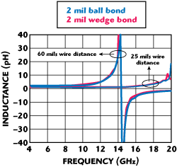
Figure 5 Measured inductance for ball and wedge bondings of the same 2 mils round wire.
Meanwhile, the wire length also affects the insertion loss directly. The measured insertion loss of the long wire shows an insertion loss 2 dB higher than that of the short wire at 20 GHz. It clearly indicates that the wiring length must be as short as possible when the operating frequency goes up above 10 GHz. The higher insertion loss is due to the impedance mismatch. In order to further compare the ball bonding and wedge bonding for the same cross-section area wires, two wires with 60 and 25 mils length were measured for comparison. From the measured results displayed in Figure 5, it is shown that two wires using ball and wedge bonding with the same cross-section have almost the same frequency response up to 20 GHz. It clearly points out that the bonding type does not affect the high-frequency performance dramatically. However, the wiring shape is the most important factor dominating the wiring characteristics.

Figure 6 Measured inductance for ribbon and wedge bonding of wires of the same cross-section area.
Ball Bonding vs. Ribbon Bonding (Same Wire Cross-Section Area)
Measurements were taken to compare the high-frequency performance between ball and ribbon bonding of wires of the same cross-section area. Therefore, a single 0.5 x 2 mils ribbon wire and double 0.8 mils round wires were measured with a spacing of 5 mils between the double round wires. Figure 6 shows the measurements for these wires with length of 75 and 45 mils. Under the same cross-section area of 1 mil2, ball bonding wires achieve lower inductance value and higher ƒSR than ribbon wire. For 75 mils wire length, the inductance values are 7.1 nH for ribbon wire and 5.0 nH for round wires; these values are 2.7 and 3.3 nH for 45 mils wire length, respectively. The lower inductance for round wires is due to the two round wires bonded in parallel, which provide a larger current flow area; therefore, the inductance values were decreased even though they have the same cross-section area as the ribbon wire. In addition, once the spacing between two round wires was increased from 5 to 10 mils, the inductance values will be reduced to 3.7 and 2.5 nH for wire lengths of 75 and 45 mils. This is because the wider spacing between the two wires generates a lower mutual inductance than the narrow spacing. However, a single 0.8 mils round wire does provide the largest inductance and the lowest ƒSR compared to the other wires, due to the smallest conductor area and significantly high-frequency parasitic effects. All the measured inductances and insertion losses are shown in Figure 7.

Figure 7 Measured inductance (a) and insertion loss (b) for ribbon and ball bonding with different wiring conditions.
The insertion losses of all wires shown, round and ribbon wires, are measured with the same wire length (60 mils). Under the same cross-section area, three types of bonding wires, 0.5 x 2 mils ribbon wire, double 0.8 mils round wire, with 5 and 10 mils separation, have almost the same ILs below 2 GHz. However, these values increase with frequency, as well as the loss difference among them. The lowest insertion loss was achieved by using double round wires with 10 mils spacing, because of their smallest wire inductance. The insertion loss of this double round wire is approximately 2 dB lower than that of single round wire at 20 GHz.
Ball Bonding vs. Ribbon Bonding (Wire Surface Area)
Measurements were performed to compare both round and ribbon wires with the same surface area, 0.5 2 mils ribbon wire with 2 mils round wire. The measured inductance results are shown in Figure 8. In this comparison, it is shown that the two wires have similar high-frequency characteristics from low frequency to 20 GHz, since the main influence is the "skin effect". However, for a DC current (zero frequency) applied to the wire, the electron flow is uniform throughout the wire. However, when a high-frequency signal is carried, the electron flow moves toward the wire surface. Therefore, due to the skin effect for the bonding wires, the same cross-section round wire has much higher current carrying capability than ribbon wire, and achieves smaller effective inductance and less signal loss. It also illustrates that the surface area of the conductor determines the current carrying ability instead of the cross-section area. To achieve the same surface area, a round wire needs more cross-section area than a ribbon wire. Moreover, this article demonstrates that the main factor dominating the wire high-frequency characteristics is the surface area of a bonding wire. Finally, all measured inductances and ƒSR results for three types of bonding wires are summarized in Table 1.
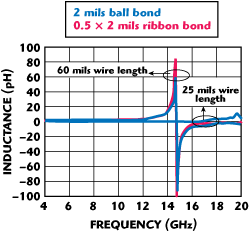
Figure 8 Measured inductance for ribbon and ball bonding of wires of the same surface area.

Conclusion
A comparison study of the high-frequency performance of ball and ribbon bonding was presented in this article. Different wire types, 0.5 2 ribbon wire, 0.8 and 2 mils round wires, were systematically measured up to 20 GHz, under two different conditions: same wire cross-section area and same surface area. The wiring self-inductance, ƒSR and IL parameters were measured. The experimental results show that the high-frequency performance for round and ribbon wires are almost identical when they have the same surface area, due to the "skin effect", and that these characteristics are quite different when the two wires have the same cross-section area. It points out that the surface area of a bonding wire mainly determines the current carrying ability, rather than the cross-section area, and dominates the electrical performance at high frequencies. This data can be very useful for RF designers when selecting the suitable bonding types for their applications.
References
- I.W. Qin, P. Reid, R.E. Werner and D. Doerr, "Automatic Wedge Bonding with Ribbon Wire for High Frequency Applications," 2002 IEEE Electronics Manufacturing Technology Symposium Digest, pp. 97-104.
- S.T. Choi, K.S. Yang, K. Tokuda and Y.H. Kim, "60 GHz Transceiver Module with Coplanar Ribbon Bonded Planar Millimeter-wave Bandpass Filter," Microwave and Optical Technology Letters, Vol. 49, No. 5, May 2007, pp. 1212-1214.
- A. Lindner, "High Speed Digital Packaging," Microwave Journal, Vol. 46, No. 5, May 2003, pp. 248-251.
- H. Izumi, H. Arai and T. Itoh, "Ribbon-wire Interconnect Using Parasitic Element," IEICE Electronics, Vol. E82-C, No. 4, April 1999, pp. 662-664.
- A.R. Mickelson, N.R. Basavanhally and Y.C. Lee, Optoelectronic Packaging, John Wiley & Sons Inc., Somerset, NJ, 1997, pp. 59-70.
- L.R. Levine, "Wire Bonding Optoelectronics Packages," Advancing Microelectronics, Vol. 29, No. 1, January-February 2002, pp. 17-19, 2002.