
Over the past five years, an explosion in growth of the portable electronics industry has provided numerous opportunities for manufacturers of RF components. Today, the designers of compact electronic systems, especially handheld/wireless devices, are faced with tightening board space constraints, thus driving the requirement for alternative integrated passive technologies. For a cell phone or PDA designer, success in the market comes from the ability to produce small handheld devices with long battery life in very high volumes. The handheld/wireless devices are attaining smaller practical size with miniaturization coming from the reduction in size of components and their associated packages. Functional integration and miniaturization is the key to this success.
To aid this miniaturization campaign, a new generation of integrated components has emerged, which offers the capability to integrate resistors, capacitors, inductors, diodes and transistors into a single monolithic device with minimal packaging overhead. By combining thin-film-on-silicon wafer fabrication technology with an advanced wafer-level chip scale packaging (CSP), dual flat no-lead (DFN) or quad flat no-lead (QFN) packaging process, component manufacturers can now provide designers with an integrated passive and active device solution that saves PCB real estate while at the same time offering remarkable electrical performance. This article discusses the thin-film-on-silicon technology used in the manufacturing of integrated passive and active devices in CSP, DFN and QFN packages. The article outlines typical functional applications including associated performance characteristics of line filtering, ESD protection, high speed bus termination, tunable filters and switching transistors.

Thin-film-on-silicon Technology
Thin film passive components have been available to the electronic designer for many years. The thin film resistors are fabricated using a tantalum nitride (TaN) layer as the resistive material and an aluminum metal layer for interconnect and contacting purposes. The aluminum metal layer and tantalum nitride layers are uppermost in the resistor construction (except for the passivation layers), while the required resistor value is arrived at using the pattern geometry (R = ?L/W) as the primary design parameter. Thin film capacitors are normally fabricated using an aluminum metal layer as the top electrode providing low parasitic resistance and inductance values for the interconnect. A silicon nitride layer is used as the dielectric and the carrier silicon substrate as the bottom electrode plate. The thin film capacitor value (C = ?A/d) represents the surface area of the top metal plate area over a lower silicon plate with a dielectric material between the plates. The thin film inductor can be constructed in a spiral or square layout where the inductor value is a function of the outer diameter, inner diameter, and number of turns and thickness of the metal layer. Inductors are fabricated using the top aluminum metal layer over a TaN layer. A lower aluminum metal layer provides the ‘lead’ into the inductor through a via-hole. Thin film resistors, capacitors and inductors are renowned for their stability, temperature characteristics and reliability. Typical thin film resistor values are in the 10 ? to 100 k? range with ±10 percent tolerance, capacitor values are in the range of 20 to 300 pF with ±20 percent tolerance, and inductors range between 1 and 15 nH, also with ±20 percent tolerance. These elements exhibit excellent performance over a broad frequency range.
Underneath the thin film layers, the silicon substrate can be used to integrate bipolar transistors and diodes of various types (Schottky, zener and varactor). These elements can be constructed on the silicon substrate using the material properties of the N or P silicon. With no board-level, copper-trace interconnections between these elements together with the most direct connection possible from component terminals to board pads, the behavior of these devices is easily controlled and highly repeatable.
Chip Scale Packaging
Given that thin-film-on-silicon integrated passive and active devices fundamentally form an integrated circuit (IC) or application-specific integrated circuit (ASIC), the package choice has, up to now, been restricted to SOIC, QSOP, TSSOP and the like. These packages have the disadvantage of being unwieldy for most space-sensitive applications and can often be counter-productive when compared to a discrete passive solution. Furthermore, the presence of bond wire parasitics renders such packages electrically unsuitable for high frequency applications. In the last few years, there has been somewhat of a revolution in the IC packaging world, where the birth of a generation of extremely space-efficient packaging solutions has been seen. Prominent among these is the wafer-level chip scale packaging process, which effectively allows individual die on silicon wafers to be “packaged” in advance of the dicing operation. The CSP uses a dual-layer dielectric system of benzocyclobutene (BCB), where the BCB layers provide an additional passivation layer on the original die surface, a planarizing dielectric coating and the definition of the solder ball wettable area. The under bump metallization (UBM) pad is constructed by sputtering Al/NiV/Cu material on the wafer and, after etching, is only present in the pad areas. For RoHS Pb-free compliance, the solder bumps use an Sn 95.5/Au 3.9/ Cu 0.6 alloy, so a solder ball is constructed on the pad and reflowed. Following singulation from the wafer, the resulting package can be considered as a “scaled-up flip-chip” component, which can be soldered directly to the printed circuit board using conventional SMT processing.
Dual/Quad Flat No-lead Packaging
Another low cost small size package that is available is the dual flat no-lead (DFN) package, which is a plastic leadless chip carrier with dual (two opposite) populated sides and an exposed thermal pad with a typical package height of 0.8 mm. All surface-mount contact pads have 100 percent Sn terminations and 0.5 mm contact pitch. This rectangular package conforms to the JEDEC package outline MO-229 and provides 4, 6 and 8 I/O options. For easier PCB routing and higher density of contact pads, the quad flat no-lead (QFN) package offers a plastic leadless chip carrier with quad (four opposite) populated sides and an exposed thermal pad with a typical package height of 0.75 mm. All surface-mount contact pads have RoHS Pb-free compliant 100 percent Sn terminations and 0.5 mm contact pitch. This square package conforms to JEDEC package outline MO-220 and provides 16 and 20 I/O options. For both package options, the singulated die is attached to the center paddle lead frame and then wire-bonded to the external I/O lead frames. The die and wire bonds are then over-molded to achieve the nominal height of 0.75 mm making them ideal for high volume SMT processing.
Cost Consideration
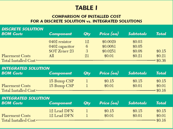
Cost is a factor that will inevitably spring to mind in the context of integrated passive and active devices. After all, thin film passive component technology has traditionally been associated with such applications as precision instrumentation, high accuracy converters and ultra-low noise amplifiers. Here, the reader may be pleasantly surprised to learn that the installed cost of a well-designed integrated passive and active device can usually compare favorably with the discrete solution that it is intended to replace. The term “installed cost” is the key. When doing the math, it is important to consider that the cost of installation does not end at the bill of materials. The main elements of the total installed cost include the price of the discrete components, the placement cost, cost of procurement and storage. The placement costs for discrete chip and/or SOT components are nearly always significantly higher than the cost of the components themselves. With this in mind, the IPAD using CSP becomes a very attractive proposition, especially when one considers the electrical and mechanical performance advantages already discussed. The costs given in Table 1 relate to the circuit in Figure 1. From this example, it is clear that there is a potential savings of nearly $0.20 per part. Additional advantages include the use of less solder paste and a reduced number of solder joints (45 for the discrete solution and 15 for the CSP solution). Furthermore, the integrated passive and active devices are electrically tested during the manufacturing process, whereas the discrete solution can only be tested once it is assembled onto the PCB.
Integrated Passive and Active Device Applications
ESD Protection
Many handheld devices have external ports, which are potential paths for ESD to enter the handheld device and damage the internal circuitry. A suitable solution for this type of problem, where board area is an issue, is an integrated passive and active device with ESD protection from contact discharges in excess of ±8 kV and air discharges of ±15 kV. For this and most handheld devices, the applicable test method is the IEC 61000-4-2 specification.
Line Termination
System bus speeds are increasing, making line termination a more important consideration. Transmission line effects, such as reflections, must be controlled to prevent misinterpretation of data or other malfunctions. Terminating bus lines using high speed Schottky diodes is an effective method in terms of both performance and cost.
ESD Protection and EMI Filters
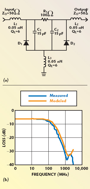
Handheld devices, such as cell phones, often have data/audio ports, which are used to connect the device to external devices such as laptop computers and headsets. Cell phones by their nature generate RF noise and this noise can be coupled into the data/audio port. Combining ESD protection and a low pass filter will attenuate the RF noise, which may otherwise interfere with the internal baseband circuitry of the cell phone. For a GSM, CMDA or 3G cell phone, some devices can offer attenuation of 30 dB minimum from 800 MHz to 3 GHz. Typically, the low pass filter is used to protect data/audio ports on wireless devices and LCD screen interfaces. A typical schematic is shown in Figure 2.
Conclusion
It is hoped that this article has shed some light on the capabilities of thin-film-on-silicon integrated passive and active devices. In particular, the intent was to demonstrate how the advent of wafer-level chip scale packaging (CSP), dual flat no-lead (DFN) and quad flat no-lead (QFN) packaging technology has made these versatile devices attractive to designers of miniature handheld wireless products by eliminating any disadvantages attributable to previous packaging forms. The integration of resistors, capacitors, inductors, diodes and transistors into single, ultra-miniature, monolithic packages has opened the door to a new level of component count reduction. This allows the bill of materials to shrink, pick and place cycles to decrease and overall product manufacturing costs to come down. In addition, manufacturers receive the advantage of reduced board real estate usage and improved electrical performance.