
Base stations use phase locked loop (PLL) systems to generate either RF or IF local signals to up-convert baseband signals to RF signals or vice versa. There are different ways of integrating PLL system blocks, including voltage-controlled oscillators (VCO), based on system requirements, performance and material cost. Why PLL performance is critical in wireless system design will be determined first, followed by a comparison of high level integrations. Detailed analytical approaches will be used to predict the baseline performance for synthesizer systems, using linear models of phase noise analysis in a closed loop, as well as overall system performance optimization, including loop filter designs.
How PLL Performances Affect Wireless Systems
Phase noise is one of the most critical impairments of radio systems, as it corrupts the information carried in the phase of the carrier due to its non-ideality. There are two different types of corruptions that phase noise can make in the systems. One is from in-band (modulated signal band) phase noise, which directly affects down converted or up converted signals, as shown in Figure 1. The amount of in-band phase noise, other than the one that is very close to the carrier, which is slow varying enough for the data to be affected, can be represented as a phase error or error vector magnitude (EVM). Another key aspect of phase noise impact can be explained with an interferer, which is often called a blocker, as shown in Figure 2. When a blocker gets up or down converted, the LO's phase noise will override its phase noise onto the blocker and parts of the phase noise will stay on top of the signal band. These types of non-ideal phase noise can impact any type of radio system such as wideband code division multiple access (W-CDMA) and global system for mobile communications (GSM). Therefore, a certain level of phase noise performance will be expected in wireless infrastructure systems.

Figure 1 Close-in phase noise impact to the incoming signal.

Figure 2 phase noise impact to the incoming signal with a blocker present.
What about long term evolution (LTE) systems? What is needed to know about LTE systems in terms of phase noise, as it becomes the next generation mobile standard? LTE uses a multi-carrier modulation technique that transmits data over a number of orthogonal sub-carriers, which consist of data and pilot within various formats of frame structures. Since orthogonal frequency division modulation (OFDM) signals transmit multi-carriers in the frequency domain, multi-carriers with the same phase noise on each carrier can be analyzed as one single-carrier with the same phase noise. However, the far-out phase noise can cause inter symbol interference (ISI), which means there is going to be a system requirement on phase noise for this system as well.

Comparison of High Level Integration for PLL Systems
Both system and component designers know why good phase noise is important in wireless systems. In this section, an approach to designing the best fitting PLL systems will be considered by demonstrating the pros and cons for each approach in designs. Table 1 shows three different integration types of PLL systems. Type 1 has one die that covers the VCO as well as PLL. This approach can be suitable for low to mid performance systems, as VCO phase noise performance will be greatly limited by low tank Q. In general, the tank Q will be limited by the Q of the inductor. Also, if a CMOS VCO is used, the 30 dB/decade slope of phase noise can be extended above 100 kHz offset, assuming the device requires high operating current and voltage swings to meet far-out phase noise performance. This will limit the usage of this type of device in low RMS phase error required systems such as higher modulation systems. It will also require off-chip loop filter components that could require great tunings to maximize the performance. Even with these performance disadvantages, the benefit comes with lower cost and smaller package size.

Figure 3 Phase noise characteristics 1.5 to 2.4 GHz CMOS cross-coupled vs. discrete BJT.
Type 2 is based on multi chip module (MCM). This type has a few dies as well as discrete components on a substrate. The die include VCO, PLL and varactors, while discrete parts include R, L, C and more. The benefit of this approach is that the VCO can have its own tank with either a low loss printed inductor using the substrate or a high Q wire wound inductor. The Q of these inductors varies from 40 to 150 depending on the size and different ways of making it. The loop filter can be either integrated or tunable outside the device. As can be expected from the high Q of the VCO tank, the phase noise performance can be quite good. If the system only requires good phase noise at high offsets—100 kHz and above—a CMOS VCO operated in high current and voltage swings could be a solution. However, if the system requires a low RMS phase error, a discrete bipolar VCO could be a better solution. Figure 3 shows a typical phase noise difference between a CMOS VCO and a bipolar VCO in Type 2 cases. In Figure 3, one can tell the difference in phase noise slope that can affect system performance.

Figure 4 Loop filter design vs. performance parameters.
Loop Filter Design and Optimization
A good loop filter design is critical for the success of a complete PLL system design, since it affects the performance of closed loop composite phase noise, spurious as well as lock time. Designers can design a specific loop bandwidth to optimize performances required for their systems. The phase margin should be above 45°, probably better than 50° to minimize the RMS phase error in the systems. Figure 4 shows the general rule of how the loop filter design can affect performance of a PLL system. This article will not discuss how the loop bandwidth or phase margin can be calculated, as this information is available in many other articles. Rather, how the Z(s) transfer function of a loop filer can be obtained, for either passive or active cases, so that designers can optimize the performance in a closed loop will be analyzed.

Figure 5 Typical passive and active loop filters.

Figure 6 Definition of the ABCD matrix and the relationship with the Z matrix.

Figure 7 Series and parallel components in an ABCD matrix.
Figure 5 shows typical passive and active loop filter circuits. Finding Z(s) should not be a big issue, if only up to 2nd order filters including R1, C1, C2 can be used in a passive filter; however, if one has to go for a higher order filter such as 3rd or even 4th or 5th order for better rejections on spurious, it will cause a headache for a designer to calculate the transfer function Z(s). Here, an ABCD matrix [F] will be used to effectively and easily find Z(s). The definition of an ABCD matrix [F] and the relationship with the Z matrix are shown in Figure 6. As one can see from the Figure, the interest is to find out 1/C, which is Z21 since it equals V2/I1, the definition of Z(s) of a loop filter. The main reason an ABCD matrix is used is that the cascaded two-port networks can simply be multiplied to calculate the combined matrix. Series and parallel components can be translated in an ABCD matrix, as shown in Figure 7, for the calculations.

Figure 8 Breakdown of each series and parallel components.
Figure 8 shows the breakdowns of each series and parallel components from the original passive and active loop filters to calculate the ABCD matrix.
If [F] is found, it will be [F] = [F1][F2][F3][F4][F5][F6] for the passive filter, and [F]= [F1][F2][F3][F4][F5][F6] [F7] for the active filter.
The complete matrix for the passive and active cases is shown here:
• Passive filter case

• Active filter case

The rest of the calculation to extract 1/C can be easily done by using any kind of engineering software such as Matlab or Mathcad. By using an ABCD matrix, finding a loop filter transfer function can be much easier as it can separate the series and parallel components as an independent unit.

Figure 9 Linear time invariant (LTI) phase domain model of a synthesizer system.
Closed Loop Phase Noise Analysis Using a Linear Model
One of the big issues in designing a PLL system is to estimate the performance by knowing how the loop will perform in terms of phase noise. The process of phase noise estimation will give a baseline performance that can be expected before the actual device is available for testing. In Figure 9, one can see each block as a noise source and how the noise contribution can be displayed as a different form of source.
For example, the reference clock, reference divider, phase frequency detector (PFD), voltage-controlled oscillator (VCO) and main divider contribute phase noise as a form of phase error. The charge pump (CP) and loop filter (LF) generate a noise source as a form of noise current and voltage. All of these noise sources can be simulated from each block of circuit and be extracted from noise simulation. As the noise source of each block is identified and quantified, finding the transfer function (TF) for each noise source will be needed to come up with a number for the phase noise at the VCO output, so that the total composite contributions from all different sources will be known.
The transfer functions can be calculated based on control system theory. Below is the TF for each block, referenced to the VCO output.
-
Reference clk, Reference buffer – [dBc]
1/R*N*open_loop/(1+open_loop) -
CP (charge pump) – RMS noise current [A]
2π/Kd*N*open_loop/(1+open_loop)-20log10(√2)
-
LPF (low pass filter) – RMS noise voltage [V]
(2πKvco/s)/(1+open_loop)-20log10(√2)
-
R, N divider, PFD (phase frequency detector), SD (sigma delta modulator) – [dBc]
N*open_loop/(1+open_loop)
Open_loop = G(s)*H(s)
G(s) = (Kd/2/π)*Z(s)*(2πKvco/s)
H(s)= 1/N

Figure 10 An example of simulated block noise source contribution to composite phase noise of a 2.1 GHz PLL system.
By multiplying the noise source to the noise TF, a composite noise level has been estimated, as well as each block's noise contribution, as shown in Figure 10. One can tell that the measured data matches the simulated composite phase noise very well. Surprisingly in this particular case, one can also tell that the major noise contributor is the low pass filter (LPF). Therefore, one can go back and check what resistor values are being used and how big the Kvco is. This analysis not only gives the estimated composite phase noise, but also gives a possible clue for the circuit block of noise source that could be a dominant noise contributor in a PLL system. The composite phase noise simulation can be compared to the measured data, when the complete PLL system is available, to increase the reliability of the simulation data compared to the measured data, even though measuring each noise block may not be easy.
Tips on Estimating and Tuning Major PLL System Specifications
Phase Noise
First, one needs to know the target phase noise specification. For example, if the system requires; -82 dBc at 1 kHz, -95 dBc at 10 kHz and -115 dBc at 100 kHz, then one should be able to plan what phase noise will be needed for each of the VCO, LPF and what noise floor will be needed on the synthesizer, so that it can be estimated if the current VCO, LPF and synthesizer have adequate phase noise margin by changing the loop BW (bandwidth) in the calculation. In general, one can set the loop BW close to where the free running VCO phase noise crosses the PLL noise floor to minimize RMS phase error. Also, one must make sure that the reference signal, either from a crystal or signal generator, is not affecting the composite phase noise.
Loop Filter Design
In general, a passive loop filter is preferred as it generates less noise compared to an active filter, since an active filter requires many active devices. However, resistors, even in a passive loop filter design, need to be carefully chosen if the VCO has a very high Kvco, since the Kvco term is in the numerator of the noise transfer function.
The loop filter components' grounding can affect the performance of the loop filter in terms of spurious and other. If one thinks the rejection of the loop filter is not enough, the layout of the loop filter components should be checked.
Spurious
If high spurious levels are seen, one must figure out whether the spurious is coming through the CP or directly coupling to the VCO output. If the spurious is coming through the CP, one should be able to reject it with the loop filter design. However, if it is from direct coupling to the VCO output, the coupling path will have to be determined to remove or lower the spur level. By increasing the loop BW, one may be able to tell if the spurious coupling is directly related to the VCO output, since the VCO noise transfer function works as a high pass filter. In general, the comparison frequency spur is the highest spurious in an Int N system and boundary and fractional spurs are the concerns in Frac N system. The performance of synthesizers regarding boundary spurs can be checked by making boundary spurs at locations close to carriers within the loop bandwidth and compare the levels. One can also check if the loop filter is rejecting spurious properly by comparing with a spurious that is outside of the loop bandwidth as well.
Frequency Pulling
Frequency pulling is a frequency change defined for a certain load condition in a VCO. In general, the load condition can be defined as a VSWR. To minimize the pulling effect, the design needs sufficient isolation between the VCO core tank and the output. One can add high reverse isolation buffer stages for this purpose.
Frequency Pushing
Frequency pushing is a rate change in free running VCO frequency, when the power supply level changes. The unit may be MHz/V. Since the injecting signal would generate side band FM modulated components, it could also be measured as the difference between the side tone to carrier power as well. Pushing could be greatly reduced by using linear drop output (LDO), as it specifies power supply rejection ratio (PSRR) as one of the main performance factors. One may check if the design SPEC needs LDO to meet the pushing specification. The down side of using LDO is that it generates a significant amount of low frequency noise that could affect the performance of the VCO up to a 100 kHz offset. Therefore, more filtering will be needed to reduce LDO noise in high performance PLL applications such as a base station.
Here is an example of how the expected side band level as well as LDO noise impact on phase noise can be calculated:
Side band dBc at VCO output
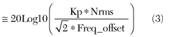
where:
Kp = pushing factor (Hz/V)
Nrms = Injected LDO RMS noise level
Freq_offset = Injected noise frequency
This equation works well as long as the peak deviation, which is the numerator in the above equation, is small enough. If an exact level of side band is wanted, one needs to use the Bessel function to find the number. Since pushing in a VCO open loop condition has been described, look at what will be different in a closed loop. The level of side band could be highest around the loop BW in a closed loop, since the VCO has a noise transfer function of high pass shape and even small gains around loop BW. With this equation, one can input any of the variables, such as side band dBc, Kp, Nrms or Freq_offset to extract any output needed.
Conclusion
Consideration has been given to how a synthesizer system can affect the overall performance of wireless systems and how a designer can choose different configurations in terms of PLL system integration. On the design side, how a loop filter transfer function can be designed by an ABCD matrix and optimized in the system was demonstrated. Also, closed loop phase noise analysis was shown to present the estimation of PLL phase noise performance by calculating noise source of each block of circuits with transfer function in a closed loop.
References
- J. Lee, "802.16e Mobile WiMAX Key RF Receiver Requirements," http://www.mwjournal.com/search/TechLib.asp?HH_ID=RES_41.
- K. Kundert, "Predicting the Phase Noise and Jitter of PLL-based Frequency Synthesizers," available at www.designer-guide.org.
Jun Lee has worked on Skyworks' CDMA2000, EVDO, WiMAX RF systems and applications and designed CDMA and EVDO single package radio (SPR) solutions. He is currently working on W-CDMA, GSM and LTE VCO circuits and phase lock loop circuits and system developments for base station applications. His current research interests include RF systems, circuits, communication theory and simulations.