
A novel design of a single-stage microwave distributed amplifier is presented in this article. The design is based on the use of a Chebyshev polynomial to express the transducer power gain of the distributed amplifier. The obtained amplifier provides a considerable increase in the bandwidth as compared to both the conventional single-stage distributed amplifier and multi-stage distributed amplifier.
Conventional MESFET distributed amplifiers (CDA) are formed by two artificial transmission lines, called gate and drain lines, actively coupled by a number of MESFET transistors.1 The gate and drain lines are made out of series inductances Lg and Ld and capacities Cg and Cd, respectively, of the MESFET transistors. In this circuit configuration, the idle ports of the gate and drain lines are terminated by the particular impedance Z0, commonly equal to 50 Ω.

Figure 1 Single-stage distributed amplifier).
The conventional single-stage distributed amplifier (CSSDA) consists of one section2-4 in which the gate and the drain line idle ports are open-circuits terminated, as shown in Figure 1. The structure is obtained from the dual-fed distributed amplifier5 in which the transducer power gain of this configuration can be improved up to 12 dB. This improvement is due to the fact that the voltage is doubled along the gate line and the recovered power will be absorbed by the loads at ports 2 and 3 within a conventional distributed amplifier structure. In this circuit, the gate line is not matched since it is open-circuited; this engenders a variable signal with frequency at the input of the transistor. The signal at the level of the load undergoes the same problem as the input signal. Unlike the CDA, the transducer power gain will oscillate within the bandwidth.
For the CSSDA amplifier, the 50 Ω matching condition of the gate and drain lines do not have meaning since both lines are open-circuited at one of their extremities. Thus, the matching constraint is raised, leading to more freedom on the choice or the determination of the gate and drain lines’ characteristic impedances, according to the wanted objectives. These characteristic impedances highly influence the circuit bandwidth. The goal that has been fixed is to look for the values of these characteristic impedances that lead to the enhancement of the bandwidth as compared to the bandwidth of the usual cases (CDA and CSSDA amplifiers) where 50 Ω is attributed to these impedances. Consequently, these characteristic impedances will serve the role of design parameters. The objective of the present work is to obtain a bandwidth at least twice as large as that obtained by CSSDA and greater than the bandwidth of the conventional distributed amplifier CDA. The amplifier with these performances has the abbreviated name of SSDA. To accomplish this, the frequency response (transducer gain) of the SSDA amplifier is approximated by a Chebyshev polynomial.5
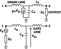
Figure 2 Equivalent circuit of the distributed amplifier).
Problem Formulation
To express the transducer power gain of the distributed amplifier, a simple unilateral MESFET model is considered, as shown in Figure 2. In this figure, Cg and Cd are the capacitor of the gate and the drain of the field effect transistor in common source configuration, respectively, and gm is its transconductance. For this structure, the transducer power gain GT is given by

where v2 and i2 are respectively the voltage and the current at the output while Eg is the internal voltage of the generator and ‘*’ represents the complex conjugate. After some mathematical development the expression of the transducer power gain becomes:

where x=  is the normalized frequency with respect to the cut-off frequency of the gate line
  while the parameters
  .
.
With  , respectively, the characteristic impedances at relatively low frequencies, of the constant-k circuits constituting the gate and the drain lines, and
  .
.
At DC signals, x = 0, the transducer power gain of the SSDA given by Equation 1 is  and the power gain of a conventional distributed amplifier of N transistors (model without gate to source and drain to source resistances) at zero frequency is given as:
  .1 The gain Gp of the conventional distributed amplifier is equal to its transducer power gain since its input is matched. The comparison between GT and Gp is valid and it shows that the SSDA amplifier has a gain equal to that of the CDA amplifier with 4 transistors (4CDA).
To approximate the transducer power gain using a Chebyshev polynomial, choose the smallest cut-off frequency among the two cut-off frequencies ωC1 and ωC2 as normalizing frequency (the frequency at which the gain starts decreasing). The choice of ωC1 as the normalizing frequency is justified by the fact that the capacitor Cg is always higher than Cd. If otherwise considered, that is ωC2 being the normalizing frequency, the gate line will start to decrease the gain at a frequency much less than ωC2, whereas the polynomial approximation results in a constant gain until that frequency. In this case, the approximation is not possible.
Dividing the gain GT by the quantity, the nomalized gain is written by the following expression:

Equation 3 contains dimensionless quantities, so it can be applied to any transistor and to any line; this in fact constitutes an important advantage. Expanding the denominator, the normalized gain of Equation 3 can be rewritten as:

where

The denominator of Equation 3 is written like  , an approximation by a polynomial of degree 8, which is the most appropriate.
To achieve the Chebyshev polynomial approximation, first the denominator of gT is written under the form of
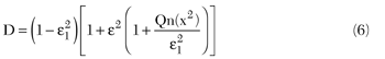
where  represents the ripple ratio, and then the approximation is carried out by using the Chebyshev polynomial Tn(x) of the terms between the brackets of the denominator D in the following manner:

The adopted form of Equation 7 results from the fact that the frequency response (the transducer gain) of the SSDA amplifier is a low pass type.
Consequently
Equations 6 and 7 indicate that gT can be greater than unity for certain frequencies within the bandwidth of the circuit. In fact, the normalized gain gT may also be written under the form of:

The variation of the transducer gain versus frequency, within the frequency bandwidth, is given as

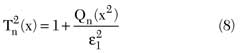
and in decibel (ΔGT)dB=10log (1+ε2)=1.3 dB, so constant regardless the values of Z0 and gm. Since Qn(x2) is of degree 8, Tn(x) must be of degree 4 and T2n(x) of degree 8:6

After identification, Equations 4 and 9 imply the following nonlinear system:
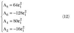
where Ai(i=2,4,6,8) are the coefficients given by Equation 5.
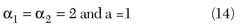
To design an SSDA amplifier, the system of Equation 12 should be first solved where the roots are α1, α2, α and ε1 (or ε). The values taken by these roots are the same, regardless of the characteristics of the field effect transistor.
Results and Discussion
The solution of system of Equation 12 gives the following:

These values are only valid for the SSDA amplifier; the following are found for the CSSDA amplifier
With the values of Equation 13 and by taking Z0 = 50 Ω , the design parameters as a function of the gate capacitance Cg may be deduced as:

The results given by Equations 13 and 15 are general and thus can be applied to any field effect transistor. It is sufficient only to know the value of Cg, the used transistor parameter, to proceed with the design of the amplifier.
The following remarks can be deduced from the obtained results:
- The field-effect transistors with a ratio
 less than 0.119 require the addition of a shunt capacitor to the drain. The added capacitor form, in combination with Cd, a new capacitor C'd such that
  . The shunt capacitor at the gate should be avoided since it leads to a reduction of the bandwidth.
The value of 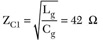 is always less than the gate and the drain lines’ characteristic impedance (Z0=50 Ω) of the CDA amplifier. This implies an increase of the cut-off frequency of the SSDA amplifier by 19 percent as compared to that of the CDA amplifier. In fact, knowing that
 , and
, and  being the cut-off frequency of CDA, thus
  . Moreover, this deviation of 19 percent is calculated by comparing the cut-off frequencies which are not defined for the same value of the gains of the SSDA and CDA amplifiers. Indeed, ωC1 of the SSDA amplifier is the frequency at which the power transducer gain starts to decrease, while that of the CDA amplifier is the value where no wave propagation exists. If the bandwidth is defined starting from DC until the frequency at which signal propagation turns off, the SSDA amplifier will yield a bandwidth larger than 19 percent with respect to that of the CDA amplifier.
Design and Simulation
The results obtained by the current approach are compared to those obtained using Microwave Office software. To accomplish this, the three amplifiers SSDA, CSSDA and 4CDA are first designed using a MESFET transistor with Cg = 0.17 pF, Cd = 0.006 pF and gm = 32mS. The calculations suggest a shunt capacitor of C = 0.014 pF to be added to the transistor drain and yield the inductances Lg = 300 pH and Ld = 653 pH for the SSDA and C = 0.164 pF and Lg = Ld = 425 pH for the CSSDA.
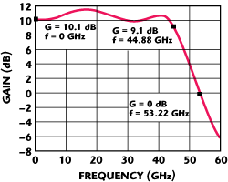
Figure 3 SSDA amplifier gain approximated by a Chebychev polynomial.

Figure 4 SSDA amplifier gain simulated by Microwave Office software.
Figure 3 shows the simulated gain GT obtained using the proposed approach and Figure 4 shows the simulated gain using Microwave Office software of the SSDA amplifier. The curves are practically the same. These figures point out the accuracy of the proposed approach. The maximum variation in dB of GT, picked up from the curves, is the same and is equal to approximately 1.3 dB, which proves the theoretical results obtained previously.

Figure 5 Normalized power gains of the 4CDA, CSSDA and SDDA amplifiers.

Figure 6 Power gains of the 4CDA, CSSDA and SSDA amplifiers simulated with Microwave Office software.
Replacing the parameters in Equation 3 by their values given by the Equations 13 and 14 and using the expression of the power gain of the CDA amplifier,1 the normalized power gain is calculated as a function of the normalized frequency for the three amplifiers SSDA, CSSDA and 4CDA. The obtained calculated gains are shown in Figure 5. The principal characteristic is that these curves are universal. It should be remarked that the SSDA amplifier, whose gain is approximated by a Chebyshev polynomial, offers a bandwidth twice as large as the CSSDA amplifier and at the same time larger than the 4CDA amplifier. Here, the bandwidth is defined as a band of frequencies in which the gain is constant or with small variations. The shape of the normalized gain curve of the 4CDA amplifier is the same as the one obtained by Moazzam and Aitchison.2,3
The curves of the power gains of the three amplifiers (SSDA, CSSDA and 4CDA) shown in Figure 6 are obtained by simulation using Microwave Office software. It is clear from this figure that if the bandwidth is defined from DC until the frequency for which the amplification ceases (gain = 0 dB), the bandwidth of the SSDA:
- Is larger than that of the 4CDA by 14.69 GHz (53.53 to 38.84 GHz). This corresponds to an increase of 39 percent, larger by 19 percent as already stated in the previous conclusion;
- Is larger than that of the CSSDA by 26.63 GHz (53.53 to 26.9 GHz). This corresponds to an increase of 98.9 percent;
The three amplifiers have the same gain in the bandwidth, which is 10.1 dB.

Figure 7 Real model of the transistor.
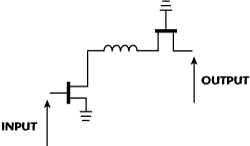
Figure 8 Cascode circuit.

Figure 9 Comparison of S12 for one transistor and a cascode circuit.

Figure 10 Comparison of S22 for one transistor and a cascode circuit.
Measurement Results
The study was done on a transistor assumed, in the bandwidth considered, unilateral and with almost an infinite capacitive output impedance value. While a real transistor does not correspond to this (see Figure 7), the circuit, which best answers the model chosen by the transistor in this study, is the cascode, in which an inductance is added between both transistors to reduce, at high frequencies, the effects of the input and the output capacity of the first and the second transistors (see Figure 8). Indeed, the curves of Figures 9 and 10 show that, contrary to the circuit with a single transistor, the cascode is practically a unilateral circuit presenting almost an infinite output impedance. The diagram of the SSDA using a cascode circuit is shown in Figure 11. Figure 12 shows the respective simulated gains of the SSDA, 4CDA and the SSDA using the cascode circuit, a real improvement of the bandwidth of the cascode compared to the other circuits.
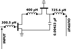
Figure 11 Diagram of the SSDA using a cascode circuit.

Figure 12 Simulated gains of the 4CDA, SSDA and the SSDA using a cascode circuit.
A comparison between the results obtained by simulation and measurements of the cascode circuit is summarized in Figure 13. The circuit was biased at 5 V drain-to-source voltage and a total drain current of 95 mA. A gain of 10.1 ±1 dB has been achieved over the 1 to 32 GHz frequency range. A photograph of the fabricated amplifier is shown in Figure 14.
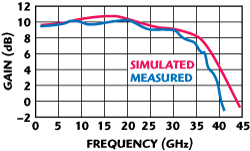
Figure 13 Comparison of the simulated and measured gains of the cascode circuit.

Figure 14 Photograph of the fabricated amplifier.
Conclusion
The proposed approach can be applicable to any MESFET transistor. The design parameters can be determined in a very simple manner since it is only sufficient to know the gate capacitance of the transistor. This approach allows significant improvement of the bandwidth of the SSDA amplifier as compared to the bandwidth of the 4CDA and CSSDA amplifiers, without any deterioration of the gain, which very often happens in the case of the conventional amplifiers.
References
- J.B. Beyer, S.N. Prasad, R.C. Becker, J.E. Nordman and G.K. Hohenwarter, "MESFET Distributed Amplifier Design Guidelines," IEEE Transactions on Microwave Theory and Techniques, Vol. 32, No. 3, March 1984, pp. 268-275.
- M.R. Moazzam and C.K. Aitchison, "A High Gain Dual-fed Single Stage Distributed Amplifier," 1994 IEEE MTT-S International Microwave Symposium Digest, Vol. III, pp. 1409-1412.
- M.R. Moazzam and C.K. Aitchison, "High-gain Microwave Amplifier Tunable Over a Decade Bandwidth," IEEE Proceedings on Microwave, Antennas and Propagation, Vol. 142, No. 6, December 1995, pp. 489-491.
- A. Worapishet, M. Chongcheawchamnan and S. Srisathit, "Broadband Amplification in CMOS Technology Using a Cascaded Single-stage Distributed Amplifier,’’ Electronics Letters, Vol. 38, No. 14, July 2002, pp. 675-676.
- C.S. Aitchison, N. Bukhar, C. Law and N. Nazoa-Ruiz, "The Dual-fed Distributed Amplifier," 1988 IEEE MTT-S International Symposium Digest, Vol. II, pp. 911-914.
- G.L. Matthaei, L. Young and E.M.T. Jones, Microwave Filters, Impedance-Matching Networks and Coupling Structures, Artech House Inc., Norwood, MA, 1980.
F. Amrani received his BS and MS degrees in electronic engineering from the University of Sciences and Technology Houari Boumediéne Bab Ezzouar (USTHB) of Algiers, Algeria, in 2005 and 2007, respectively. He is currently preparing for his doctorate degree in electronic engineering in the department of electronic engineering at the National Polytechnic School of Algiers, Algeria.
M. Trabelsi received his BS, MS and doctorate degrees in electronic engineering from the National Polytechnic School of Algiers, Algeria, in 1976, 1988 and 2002, respectively. He is currently a professor in the department of electronic engineering at the National Polytechnic School of Algiers, Algeria.
R. Aksas received his BS, MS and doctorate degrees in electronic engineering from the National Polytechnic School of Algiers, Algeria, in 1976, 1982 and 1995, respectively. He is currently a professor in the department of electronic engineering at the National Polytechnic School of Algiers, Algeria.
A. Azrar received his BS degree in electrical engineering from the National Institute of Electricity and Electronics of Boumerdes, Algeria, and his MS and doctorate degrees in the same field from the National Polytechnic School of El-Harrach, Algeria, in 1995 and 1998, respectively. He is currently a senior lecturer in the department of electrical and electronic engineering, faculty of engineering, University Mohame d Bougara, Boumerdes, Algeria.