
 Introduction to a power amplifier designed to initiate a shift in handset power amplifier technology from GaAs to CMOS
 CMOS power amplifiers (PA) are prevalent in today's WiFi and Bluetooth markets, yet extensive industry-wide development efforts for CMOS PAs for 2G and 3G mobile handsets have so far failed to yield a product that met the performance of incumbent GaAs PAs. However, a new CMOS PA from Javelin Semiconductor, the JAV5001, promises to outperform existing solutions with a patented power combiner that delivers the lowest average current under real world 3G operating conditions. The JAV5001 also features a "bandpass" PA architecture, which produces over 10 dB lower noise and includes attenuation outside the band of interest that can enable the Tx SAW filter to be removed on some mobile handset platforms. By outperforming conventional GaAs PAs and providing virtually unlimited manufacturing capacity, the JAV5001 represents a breakthrough in the industry that could initiate the long-anticipated shift in handset PA technology from GaAs to CMOS.
Growth of CMOS in 3G Handsets
Approximately ten years ago, the world's first 3G mobile handsets appeared on the market. Though the digital baseband processor was implemented in a standard CMOS process, the analog functions, including the various radio transceivers and amplifiers, were implemented in custom processes such as SiGe or GaAs. Since that time, CMOS has been steadily growing toward the antenna, as shown in Figure 1. Today, CMOS is the dominant process of choice for Bluetooth, WLAN and other peripheral radios in the handset.
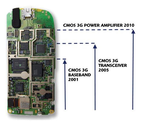
Figure 1 Growth of CMOS in 3G mobile handsets.
There are multiple reasons for the growth of CMOS. Baseband platform vendors improve economies of scale by driving as many chips as possible in the same foundry. Furthermore, GaAs PAs run on more expensive and smaller volume foundry lines. Standard CMOS foundries ensure high quality and reliable supply, which is particularly important to a market that is often subject to allocation during peak demand cycles. Additionally, CMOS enables architectural innovations and key product features not possible with custom processes that have limited digital circuitry.
CMOS PA Challenges
While the PA has long been a major opportunity for CMOS, the technical challenges have been notoriously difficult to overcome. The first concern is the belief that CMOS transistors were not fast enough to support high frequency, low noise operation. In 2005, after the ramp of the Aero transceiver from Silicon Labs into a $250 M business quieted those concerns, the attention turned to breakdown voltage limitations of CMOS. In 2007, Axiom's GSM/GPRS PA showed that those voltages could be effectively managed using a clever architecture implemented in CMOS, but the product fell short on efficiency performance. The Silicon Labs GSM/GPRS PA marked a similar achievement in the laboratory, but also fell short on efficiency.
The structure of the 3G network presents an excellent opportunity for CMOS PAs. Unlike the 2G GSM/EDGE network, the 3G network requires the mobile handset transmit power to be very accurately controlled over a wide range from -50 to +24 dBm. The PA is expected to maintain efficiency over the entire range of output power, not just at maximum power. Furthermore, the power must be highly accurate over temperature, voltage, frequency and output load impedance. These system requirements force new types of PA circuit architectures and designs to be considered for a 3G CMOS PA to achieve best-in-class performance, as well a focus on device modeling and simulation.

Figure 2 Mobile handset block diagram including JAV5001 PA.
W-CDMA Mobile Handset Example Block Diagram
Figure 2 shows a block diagram of a single W-CDMA band of a mobile handset including the JAV5001 PA. The signal is transmitted and received by the transceiver and baseband (XCVR/BB). To minimize noise in the system, the transmitted signal is filtered by the Tx SAW before it is amplified by the PA. The coupler passes a weak version of the transmitted signal that is detected and used by the baseband for transmitter power control. The duplexer provides additional filtering in both the transmit and receive paths of the signal before it is connected to the antenna switch. The JAV5001 PA integrates complete circuitry for power regulation, PA bias, input and output matching, and power control.
ACLR, EVM and PCDE Measurements
While amplifying the signal, the PA must maintain strict linearity requirements. Signal distortion for W-CDMA is measured by adjacent channel leakage ratio (ACLR), error vector magnitude (EVM) and peak code domain error (PCDE). Typical ACLRs reach better than -40 dBc (ACLR1) or -55 dBc (ACLR2) at +24 dBm of handset output power. The EVM is typically around 4 percent and the PCDE is -33 dB, providing significant margin to the 3GPP specifications (see Figure 3).

Figure 3 ACLR, EVM and PCDE measurements in a commercially available smartphone.

Figure 4 Average PA current calculated from the GSMA DG.09 usage model.
PA Current Consumption
While maintaining linearity, the PA consumes significant current that has a direct impact on the talk time, standby time and battery life of the mobile handset. The actual average current consumed by the PA depends on where and how the handset is used. Today's 3G handsets and data cards operate occasionally at maximum power, but spend most of the time at medium and low output power levels. The PA average current is calculated by multiplying currents over all output power levels by a usage profile and summing the results. Each mobile handset operator develops its own usage profile based on histograms of output power measurements from handsets or data cards in the field. The standard profile used to benchmark W-CDMA PAs is published in the GSM Association official document DG.09 entitled "Battery Life Measurement Technique." Over this usage profile, typical PA average currents range from 30 to 40 mA, as shown in Figure 4. The JAV5001 features a unique integrated power combiner that delivers a low average current of less than 27 mA.
Bandpass PA Architecture
PA noise is an often-overlooked but critically-important parameter that impacts receiver sensitivity for W-CDMA and also for other systems in the handset such as Bluetooth or GPS. Unlike the GSM/EDGE 2G system, which is time division duplex, W-CDMA is a full duplex system, which means the mobile handset receives signal while its transmitter is turned on. To get a feel for the numbers, the W-CDMA receiver is typically specified to receive signals as low as -110 dBm at the antenna while the W-CDMA transmitter operates at 24 dBm. In practice the PA may operate as high as 28 dBm to overcome the front-end losses, which means that large isolation of around 138 dB between the PA output power and the receiver signal must be achieved. Furthermore, receivers for GPS and Bluetooth can be active during W-CDMA transmit, which places additional limitations on the W-CDMA transmitter power.
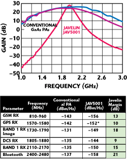
Figure 5 Javelin's bandpass PA architecture includes the function of the TX SAW filter.
The strategy employed in the handset is to filter out the unwanted W-CDMA power that leaks from the transmitter into the receiver frequency bands. Typically, the Tx SAW provides about 35 dB of filtering, but also reduces the signal by about 2 dB due to insertion loss. However, the Tx SAW filtering is counteracted by the PA gain. For conventional PAs, the counteraction is significant. For example, at the GPS frequency of 1575 MHz, conventional PAs provide 25 dB of gain. An alternative architecture, employed by the JAV5001 CMOS 3G PA, is to create a "bandpass" PA response, which provides significant attenuation outside the band of interest. At 1575 MHz, the JAV5001 attenuates the signal by 8 dB, corresponding to 33 dB of rejection compared to a conventional PA. This response essentially mimics the rejection of the Tx SAW filter and can enable it to be removed. Removing the Tx SAW not only saves the system bill of materials, but it also saves Tx current by allowing the transceiver and PA to operate at lower output powers. Figure 5 shows the gain measurements.
Industry-standard Footprint
Today's PAs are converging to a 3 x 3 mm package for single band designs. The JAV5001 is already implemented in a standard 3 x 3 mm footprint. The PA uses an industry standard digital power control using two mode pins.

Figure 6 The JAV5001 is implemented in a standard 3 x 3 mm package and requires only two external components.
The wireless industry has long enjoyed the benefits of CMOS solutions in Bluetooth and WLAN products, as well as in the baseband and transceiver portions of 2G/3G cellular handsets. After years of research and failed attempts, a power amplifier has finally been developed in CMOS that meets the stringent performance requirements, and outperforms the GaAs incumbents. Javelin Semiconductor's JAV5001 is the first product in a family of high performance 3G CMOS PAs to address the fast growing 3G mobile handset market. As RF complexity continues to increase in the mobile handset, including multiple frequencies, band sharing and multimode requirements, the JAV5001 represents a core technology that can initiate the long-anticipated industry shift from GaAs to CMOS.
Javelin Semiconductor,
Austin, TX
(512) 684-6350,
sales@javelinsemi.com,
www.javelinsemi.com.
RS No. 300