
In order to obtain circular polarization, a dual feed can be used to excite a square patch to generate two fundamental modes, TM10 and TM01, radiating at the same frequency. To meet the necessary conditions for circular polarization, the two modes must be equal in magnitude and ±90° out of phase. Hence, an external polarizer in the form of a power splitter or a directional coupler has to be used and, consequently, the board space of the antenna is increased.1 A more compact form of the antenna can be obtained by using a single probe feed to excite a nearly square patch.2 The area of the perturbation segment must be carefully determined so that the fundamental mode is split into two degenerate modes (TM10 and TM01) radiating at two slightly different frequencies and also satisfy the conditions for circular polarization. The single feed is normally located along one diagonal to produce left-hand (LH) circular polarization or along the other diagonal to produce right-hand (RH) circular polarization.3 For the diagonal feed, the area of the perturbation segment is small so that the two dimensions (a and b) of the nearly square patch are approximately equal and hence are very sensitive to manufacturing errors. It is shown in this article that, by using a single microstrip feed, offset from the corner and along one edge of the nearly square patch, the area of the perturbation segment is increased. Further increase in the area of the perturbation segment can be obtained by using a thicker substrate. Consequently, the effect of the manufacturing errors on the performance of the antenna is further reduced.
To simplify the design of this antenna, an equivalent circuit is derived. The radiation along the edges of the patch of the two modes is modeled by two parallel tuned circuits, which are connected to the feed point by two transformers. Based on this equivalent circuit the dimensions of the patch are obtained so that the antenna operates at the designed frequency. Finally, to match the complex input impedance of the antenna to Z0, a short length of microstrip line is used.
Equivalent Circuit Derivation and Design of the Antenna
Figure 1 shows a nearly square patch antenna having physical dimensions a and b with b > a. The patch is normally fed along one of the two diagonals to generate either RH or LH circular polarization. The area of the perturbation segment (?S) must be such that the two modes satisfy the conditions for circular polarization as shown. The problem with the diagonal feed is that ?S is very small.

Fig. 1 Single diagonal feed CP patch antenna; (a) nearly square patch, and (b) amplitude and phase of the two modes.

Fig. 2 Single offset feed CP patch antenna; (a) nearly square patch with probe field, (b) its equivalent circuit, and (c) nearly square patch with microstrip feed.
More generally, it has been shown2 that circular polarization can also be achieved by a probe feed located at any point on a locus (x0, y0), as shown in Figure 2 for RHCP and LHCP when the patch dimensions depend on the probe location. The equivalent circuit of the antenna where the two tuned circuits represent the two radiating modes at the edges of the patch is also shown. The two transformers Ta and Tb with turns ratio Na and Nb transform the two edge impedances to the feed point (x0, y0). For the TM10 mode, the voltage VFa along the ‘a’ edge of the antenna is proportional to Va cos(?x0/a), while for the TM01 mode, the voltage VFb along the ‘b’ edge is proportional to Vb cos(?y0/b). The turns ratio Na is VFa/Va ? cos (?x0/a) and similarly Nb is VFb/Vb ? cos(?y0/b). Therefore, the ratio Nb/Na is given by

From the circuit, it can be shown that, for CP, the ratio Vb/Va is given by
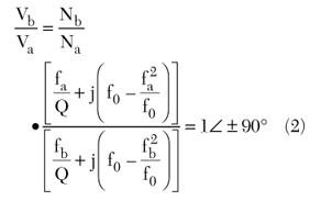
where
f0 = design frequency
fa and fb = frequencies of the two modes
Q = Q-factor of the patch
The frequencies for the two modes are given by
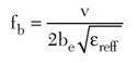
and

therefore

where the physical dimensions a = ae – 2?a and b = be – 2?b, ae and be are the effective dimensions of the patch, v is the velocity of light and ereff is the effective dielectric constant. To determine accurately Da and Db due to the fringing effect, it is recommended that the equations given in Reference 4 be used.
Substituting Equation 3 into Equation 2 for fa and applying the CP conditions gives the following results:
For the magnitude condition, it can be shown that

where

Similarly for the phase condition:

Equations 4 and 5 are solved to determine the values of the effective patch dimensions ae and be for a given feed location (x0,y0). The value of Q can be determined for the unperturbed square patch,5 or by simulation,6 or by practical measurement at the design frequency f0.
An antenna with a microstrip feed is easier to match than one with a probe feed. The design presented here is for a feed position (x0,0) as shown in the figure, so that

Effect of the Microstrip Offset Feed Position and Q on the Size of the Perturbation Segment
Solving Equations 4 and 5, the percentage of the perturbation ?Se/Se as a function of the offset feed position x0 with a fixed y0 = 0 and Q are shown in Figure 3. As can be seen for the corner-feed position at x0 = 0 and y0 = 0 the area of the perturbation segment is very small and the condition for circular polarization is very sensitive to manufacturing errors. As the offset feed position x0 approaches the center of side a, the percentage of ?Se/Se increases exponentially. By using a thicker substrate, the Q-factor of the patch is reduced, which further increases the relative size of ?Se/Se.

Fig. 3 ?Se/Se perturbation versus offset feed position and Q-factor.
Input impedance and matching
For a square patch using an FR4 PCB substrate with ?r = 4.3, h = 1.575 mm, tan ? = 0.019, and at an operating frequency of 2.45 GHz, the calculated value of Q was 32.7. The input impedance of the antenna at the offset position x0, and y0 = 0 is given by5

where

w = width of the feed line
It is sufficiently accurate, for values of Q < 35, to use only the first five terms of the series to calculate Zin.
For offset feed positions in the interval 0 ? x0 ? 0.45a, the dimensions of the nearly square patch were determined using Equations 4 and 5, and Zin obtained from Equation 6.
The predicted input impedance Zin is compared with simulation results, as shown in Figure 4. As x0 approaches 0.5a, Zin becomes smaller, making it very difficult to match the antenna. Consequently, in the realization of the matching network, there is a trade-off between the increase in perturbation and the feed location.

Fig. 4 Calculated and simulated Zin as a function of the offset factor.
To maintain a compact form of the matched antenna, a short length of a microstrip line is used, as shown in Figure 5. The transmission line model of the matching network is also shown.

Fig. 5 Matched CP antenna (a) configuration and (b) transmission line matching network.
The characteristic impedance Z0m of the microstrip line is given by7

where Z0 = 50 ? and Zin = R + jX is the input impedance of the patch.
The electrical length of the matching line is given by

By this method, only a certain range of Zin can be matched, as shown in Figure 6, and this determines the maximum value of the offset position x0.

Fig. 6 Region of Zin that can be matched using the matching network.
Simulated and Measured Results
A nearly square patch antenna was designed with the offset feed location at 0.3a. The calculated and simulated input impedances of the patch were 97–j35.4 ? and 75.5–j32.2 ?, respectively. The design of the matching network was based on the input impedance of 75.5–j32.2 ?. The parameters of the designed antenna operating at 2.45 GHz are summarized in Table 1. The fabricated nearly square patch antenna with a simple matching network is shown in Figure 7.


Fig. 7 CP, nearly square patch antenna fabricated on FR4 PDB substrate.
Figure 8 shows a comparison of the simulated and measured results for the axial ratio (AR) of the designed antenna. The measured axial ratio was 0.45 dB at 2.458 GHz, which is less than a 0.5 percent shift from the design frequency. The simulated and measured results for the return loss also show good agreement.

Fig. 8 CP patch antenna’s (a,b) axial ratio and (c) return loss.
Conclusion
Based on the equivalent circuit of the nearly square patch antenna, the conditions for circular polarization were determined. It has been shown that using an offset microstrip line and a thicker substrate increases the size of the perturbing segment. To match the antenna a simple matching network has been designed, consisting of a short length of microstrip line. The measured and simulated results are in good agreement with predicted values.
Acknowledgment
The authors would like to acknowledge the assistance of Peter Gale, Peter Elsdon, Stan Scott and professor Fary Z. Ghassemlooy.
References
- J.Q. Howell, “Microstrip Antennas,” IEEE Transactions on Antennas and Propagation, Vol. 23, No. 1, January 1975, pp. 90–93.
- M.I. Aksun, S.L. Chuang and Y.T. Lo, “On Slot-coupled Microstrip Antennas and Their Applications to CP Operation — Theory and Experiment,” IEEE Transactions on Antennas and Propagation, Vol. 38, No. 8, August 1990, pp. 1224–1230.
- M. Haneishi and S. Yoshida, “A Design Method of a Circularly Polarized Rectangular Microstrip Antenna by One-point Feed,” Electronics and Communications in Japan, Vol. 64-B, No. 4, 1981, pp. 46–54.
- M. Kirschning, R.H. Jansen and N.H.L. Koster, “Accurate Model for Open End Effect of Microstrip Lines,” Electronics Letters, Vol. 17, No. 3, 5th February 1981, pp. 123–125.
- E.G. Lim, “Circular Polarised Microstrip Antenna Design Using Segmental Methods,” PhD Thesis, University of Northumbria at Newcastle, UK, May 2002.
- Ansoft Ensemble v8, Ansoft Corp., 2001.
- H.A. Atwater, “Reflection Coefficient Transformations for Phase-shift Circuits,” IEEE Transactions on Microwave Theory and Techniques, Vol. 28, No. 6, June 1980, pp. 563–568.