
Miniaturization and cost reduction along with ever expanding user functions are important features for modern consumer communication devices as customers demand more data throughput at low cost. System-on-chip (SoC) and system-in-package (SiP) have brought more and more circuits and functions together. For passive circuits, traditional multi-layer printed circuit boards (PCB) not only function as a carrier for packaged, or bare-chip integrated circuits and surface-mount components, but also provide for interconnect and some incorporation of passive elements and circuits.1–2 In recent years, low temperature co-fired ceramic (LTCC) has become popular for passive circuit integration due to its higher integration capability, better temperature handling and lower dielectric loss. When using screen-printed silver paste, the conductor loss for LTCC is comparable with copper-based PCB. LTCC is employed in cellular phone front-end modules, matching circuits for power devices, IC interposers, etc. However, due to the process limitations of screen printing, metal line width and spacing is limited to approximately 50 µm. Also, in order to provide sufficient physical strength and avoid substrate warpage during firing, the total LTCC thickness generally needs to be greater than 400 µm.
Today there is a continually increasing demand for thinner and more functional per unit area substrates, which pushes the LTCC technology to uncomfortable limits. In this situation, a thin-film approach using photolithography technology is becoming a preferred way to meet this demand. Thin-film processes have been used in the semiconductor industry for decades and, therefore, the technology is mature. However, it is generally more expensive than LTCC and PCB when used for passive circuits. In order to be competitive in cost and performance with LTCC, suitable thin-film passive (TFP) processes need to be established. First, compared with semiconductor thin-film, TFP circuits do not have active devices, and consequently do not require multi-million dollar, sub-micron resolution steppers. In most cases a process accuracy of a couple of microns is sufficient for TFP, which significantly reduces the equipment and mask costs. Second, using lower grade substrates, without the strict surface smoothness and epitaxial layer requirements, can potentially reduce material costs. Keep in mind that in order to reduce transmission line and inductor losses, low dissipation factor dielectric substrates still need to be used. Suitable dielectric materials include alumina, low grade GaAs, high resistivity Si, Si coated with SiO2, sapphire, quartz, and other proprietary materials and ceramics. In addition, high conductivity metals up to a few skin depths thick at the lowest application frequency need to be used.
In this article, a dual-band wireless local area network (WLAN) antenna switching module (ASM), employing transmit (Tx) and receive (Rx) diplexers combined with a gallium arsenide (GaAs) switch, is designed and fabricated using thin-film passive technology. A low dielectric constant ceramic is chosen as the substrate material. Size and performance to a comparable LTCC component is presented. Methods of improving the inductor Q by metal selection and design are also discussed.
For TFP circuitry, inductor and transmission line losses are the dominant factors for total circuit loss since capacitors normally have ten times higher Qs than inductors. Hence, the optimization of the inductor Q is a primary target when establishing a thin-film passive process. Significant factors dramatically affecting inductance and Q values include metal conductivity, metal layer thickness, substrate loss, inductor shape and structure. The conductivity of the metal is usually the most significant factor since it accounts for most of the thin-film inductor loss.3
Minimizing Inductor Loss
Figure 1 shows the cross-section of a thin-film passive device. The substrate used is alumina for low cost and low microwave loss. The first metal layer is made of 2.4 µm thick copper (Cu) chosen for its high conductivity and, therefore, offers high inductor quality factor. The capacitors are made using a 0.1 µm thick Si3N4 dielectric layer. Three micron-thick polyimide is used for inductor bridges and isolation from the first metal. The second metal layer is 3.4 µm thick gold (Au), which is good for pad connection and protection of the Cu layers that are not stable in open air.

Fig. 1 Thin-film passive device substrate cross-section.
Figure 2 shows the effect of both copper and gold metal conductivity on inductor Q for a 7-turn inductor. It can be seen that despite the same size and geometry, the copper inductor has 22 percent higher Q than a gold inductor at 2 GHz. There is good agreement between the measured and simulated results.

Fig. 2 Effect of metal conductivity on inductor Q.
Figure 3 plots the results of simulations looking at the effect of substrate loss (dissipation factor) on inductor Q. It can be seen that the substrate loss becomes pronounced only after the loss tangent is greater than 0.01 assuming typical copper metal losses. This means that as long as the loss tangent factor is less than 0.01, the dielectric loss has a limited effect on total inductor Q.
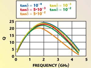
Fig. 3 Effect of substrate dissipation factor on inductor Q.
The effect of Cu metal thickness on inductor Q is shown in Figure 4. The inductor Q improves rapidly over all frequencies with thicknesses increasing from 1 to 2 µm. From 2 to 3 µm, the Q improvement happens mainly at lower frequencies due to the critical skin-depth requirements being met. From 3 to 5 µm, the Q improvement at low frequencies becomes less pronounced but the peak Q starts to decrease due to increased turn-to-turn coupling. Thus, an optimum Q is achieved at a Cu thickness of approximately 3 µm.
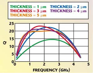
Fig. 4 Effect of the metal thickness on inductor Q.
The design guides in Figure 5 were generated to help in selecting the most suitable inductor size and shape in order to maximize the Q at a given frequency. It includes inductors of different line width, line spacing and core sizes. It can be seen that inductors with a bigger core size, or occupying a larger area, tend to have higher Qs. A designer can compromise among Q, size and shape for a particular application. For the remainder of this article, inductors with a metal width and spacing of 15 µm are used.

Fig. 5 Inductor design curves.
TFP and LTCC Comparison
Thin-film filters offer large size reductions when compared with LTCC parts. In bandpass filter and diplexer examples with similar circuit topologies, thin-film parts are five to seven times smaller than their LTCC counterparts, with a comparison shown in Figure 6. From an insertion loss perspective, LTCC filters have lower loss. LTCC inductors are normally fabricated using screen-printed silver paste with a cured thickness of approximately 10 µm and have bigger geometries and total volume than their thin-film counterparts. This gives them a Q in the range of 40 to 60, larger than the 20 to 25 seen in thin-film inductors. Thus, if using a similar circuit topology for a bandpass filter, LTCC parts will have approximately 0.5 dB lower insertion loss at 2 GHz and 0.3 dB lower at 5 GHz (see Figure 7).

Fig. 6 TFP and LTCC size comparison for a WLAN diplexer example.
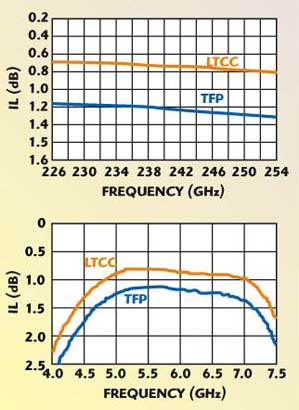
Fig. 7 TFP and LTCC insertion loss (IL) comparison for a WLAN diplexer example.
TFP ASM Performance
The photograph in Figure 8 and block diagram in Figure 9 are for a prototype WLAN antenna switch module consisting of two diplexers, Rx and Tx, and a GaAs antenna diversity switch. The RF inputs and outputs are connected by coplanar waveguide (CPW) ports for probing, while the DC controls are connected by bond wires. The size of this circuit is 2.1 × 2.0 mm2 when the port area is excluded.

Fig. 8 A TFP WLAN antenna switch module.

Fig. 9 Block diagram of the TFP WLAN antenna switch module.
Each diplexer is made up of a low pass filter and a bandpass filter, as shown in the schematic of Figure 10. Four 15 pF DC blocking capacitors are included on the chip for the switch. The Tx and Rx diplexers are simulated using 2.5 dimensional electromagnetic software, with performance verified on separate samples, so that the ASM’s Tx and Rx channel performance can be analyzed without any stray coupling. The S-parameters provided by the switch manufacturer are used to simulate the switch. Figures 11 and 12 show the ASM Rx and Tx channel insertion loss performance together with that of the diplexers. It can be seen that the total loss agrees well with the sums of the sub-circuits losses, which indicates that the ASM sub-circuits match each other well. Compared with the size of an LTCC part of similar configuration,4 measured as 10.4 × 3.3 mm2, this TFP design is about an eighth that of an LTCC part.

Fig. 10 Circuit diagram of a 2 and 5 GHz diplexer.

Fig. 11 Antenna switch module Rx channel loss.

Fig. 12 Antenna switch module Tx channel loss.
Conclusion
In this article, a thin-film passive antenna switch module has been developed on a low loss ceramic substrate. Copper was selected for the inductor metallization in order to increase the inductor Q. A comparison between the TFP process and LTCC process as well as design methodologies for inductors have been discussed. Loss analysis of the ASM shows that good module performance has been achieved.
Acknowledgment
The authors would like to acknowledge the assistance of Bryan Farber for assembling and testing the ASM.
References
- “Integrated Passives – A Quantitative Case Study,” The Prismark Wireless Technology Report February 2004, Prismark Partners LLC.
- “Three Generations of Freescale Transmit Modules,” Prismark Wireless Technology Report September 2004, Prismark Partners LLC.
- I. Bahl, “Lumped Elements for RF and Microwave Circuits,” Artech House Inc., Norwood, MA, 2003.
- N. Mellen, R. Chen, J. Horne and H. Patterson, “WLAN RF Module Design Tradeoffs,” 2004 IEEE MTT-S IMS Workshop WSA: Wireless-LAN Solutions and RF Front-end Integration Trends, Fort Worth, TX, June 2004.