
In this article, a new Doherty amplifier using high-efficiency inverse class F and class F amplifiers is presented. The characteristics of inverse class F and class F amplifiers have been analyzed for their bias conditions and load impedances in order to identify their suitability to be the carrier or peaking amplifier in a Doherty amplifier. An inverse class F amplifier was employed for the carrier amplifier due to its superior linearity and efficiency performance over a wide range of load impedances. The class F amplifier was used for the peaking amplifier by virtue of its larger gain expansion characteristics. The proposed Doherty amplifier was configured using the implemented inverse class F and class F amplifiers for the 1 GHz band and evaluated using two-tone and down-link WCDMA signals. A state-of-the-art efficiency performance was achieved at a given linearity level: A power-added efficiency of 50.9 percent at a third-order intermodulation distortion level of -30 dBc from the two-tone test and 45.2 percent at an adjacent leakage power ratio of -30 dBc from the WCDMA test, respectively.
Wide-band signals with a high peak-to-average ratio (PAR) have been extensively adopted in modern wireless communication systems. For radio-frequency circuit designers, the efficiency versus linearity trade-off turns into one of the most important design considerations. Doherty amplifiers, which employ a load impedance modulation technique, have been adopted for use in base station power amplifiers due to their simple structure, good linearity and high efficiency at average output power levels.1-6 For high efficiency, various class F and inverse class F (or class F-1) amplifiers have been analyzed and implemented. Most of the previous work regarding class F or class F-1 amplifiers has been designed to enhance efficiency.7-9 However, these amplifiers inherently have poor linearity due to excessive harmonics in the voltage or current waveforms.10
S. Goto, et al proposed a Doherty amplifier with a combination of class F and inverse class F amplifiers.11 They reported high efficiency at an output power back-off of 10 dB for two-tone excitation. However, the efficiency and linearity rapidly degraded after the peak point, which can result in significant performance degradation for the signals having much higher peak-to-average power ratio (PAR or PAPR), such as the down-link wide-band code division multiple access (WCDMA) signals. J. Kim, et al proposed a saturated Doherty amplifier using class F amplifiers.12 They reported very high efficiency but poor linearity. For the WCDMA signal, the reported performance could not come down to an adjacent channel leakage power ratio (ACLR) of -30 dBc. The ACLR performance got even worse for the lower output power level.
In this article, a new Doherty amplifier using class F and F-1 amplifiers is proposed. Various possible configurations for the Doherty amplifier were compared with each other, using circuit simulations for a high-power transistor. Based on the simulation and analysis results, it was determined that the performance of the Doherty amplifier can be significantly improved using class F-1 as the carrier and class F as the peaking amplifier cell, while the conventional configuration deploys class AB for the carrier and class B for the peaking amplifier. The proposed configuration is exactly opposite to that of S. Goto, et al.11
The proposed configuration of the Doherty amplifier was implemented and evaluated for the 1 GHz band using two-tone and down-link WCDMA signals. The measured performance of the proposed Doherty amplifier was compared with a balanced configuration using the same amplifier circuits.
The Class F and F-1 Amplifiers
An ideal class F amplifier is required to have a half-sine current waveform, containing even harmonics, and a square voltage waveform, containing odd harmonics. Meanwhile, an ideal class F-1 amplifier is required to have a half-sine voltage waveform and a square current waveform. The efficiency of the class F and F-1 amplifiers has been well investigated in many previous research efforts, but the linearity of both amplifiers has not been seriously taken into account. To maximize efficiency, both amplifiers are mostly biased to the class B or C point and terminated with optimized impedances so that the highest power-added efficiency (PAE) can be extracted. However, the highly truncated current waveform, which contains abundant harmonics, ruins the linearity performance of the class F and F-1 amplifiers.
The bias point of the class F and F-1 amplifiers can be raised from class B or C toward AB so that they have appropriate harmonic current and voltage levels for better linearity. The fundamental impedance should also be tuned not only for efficiency but also for linearity. In order to gain high efficiency and good linearity at the same time, the class F and F-1 amplifiers were biased to a class AB and the fundamental impedance was optimized for the best compromised efficiency and linearity.

Figure 1 Output circuit diagrams including harmonic control networks: (a)class F amplifier and (b) class F-1 amplifier.
The output networks of the class F and F-1 amplifiers are shown in Figure 1. Because the high-power transistors include significant internal parasitic components, the second and third harmonic control circuits should be located right after the transistor and properly tuned for both amplifiers.7 A λ/4 short-stub transmission line was used for both the second harmonic control and drain bias feed and a λ/12 open stub transmission line was used for the third harmonic control. Afterward, the low pass fundamental matching network followed and transformed the optimum fundamental load impedance to a 50Ω load.

Figure 2 Simulated output voltage and current of the class F amplifier at peak power added efficiency: (a) spectra and (b) waveforms.

Figure 3 The simulated output voltage and current of the class F-1 amplifier at the peak PAE point: (a) spectrum and (b) waveform.
For design validation, a harmonic balance simulation was carried out for both amplifiers. The amplifiers were designed using Freescale’s MRF281S, a 4 W laterally diffused metal-oxide-semiconductor field effect transistor (LDMOS FET). Since the class F amplifier had the second harmonic impedance shorted and the third harmonic impedance open, the drain current peaking for the second harmonic frequency band and drain voltage peaking for the third harmonic frequency band could be successfully achieved, as shown in Figure 2. For a class F-1 amplifier, the second harmonic voltage peaking and the third harmonic current peaking were clearly observed from Figure 3. The resultant time domain current and voltage waveforms are also shown in the figures for class F and F-1 amplifiers, respectively.
Table 1 summarizes the simulated and experimental performances of class F and F-1 amplifiers, where parantheses indicates a measured value. These amplifiers are all biased at the same class AB point (IDQ = 25 mA). For the two-tone test, the data was extracted at an IMD3 of -30 dBc. The simulated performance of the conventional class AB amplifier is also presented for comparison. For two-tone excitation, the performance of class F and F-1 amplifiers exhibit comparable efficiencies and a little higher output power at a given third-order intermodulation distortion (IMD3) requirement of -30 dBc. In addition, the peak PAEs are improved by as much as 4.5 and 8.1 percent for the class F and F-1 amplifiers, respectively. Consequently, a comparable linearity and much higher peak PAEs were achieved using class AB biased class F and F-1 amplifiers, when compared to the conventional class AB amplifier.

The Configuration of the New Doherty Amplifier
The Peaking Amplifier
In the configuration for the Doherty amplifier, the peaking amplifier is generally biased to a class B or C point for two main reasons, while the carrier amplifier is generally biased to a class AB point. First, this low bias could be used to improve linearity: The third-order intermodulation current of the class B or C amplifier has an opposite phase to the class AB amplifier. Hence, the resultant IMD3 can be improved.
Second, this low bias of the peaking amplifier ensures a correct load modulation in the low power region. Because the peaking amplifier should be turned off in a low power region and supply the same current to the load at a high power level, its gain expansion should be high enough. The sufficiently large gain expansion, which allows it to have a proper ON/OFF transition according to the output power level, is thus a very desirable characteristic for a peaking amplifier.
Therefore, an analysis for the gain expansion of the class F and F-1 amplifiers was performed in detail. An output current for the weakly nonlinear current source in general common source amplifiers can be expressed using the Taylor series expansion:
.gif)
where vg(t) is an input signal. The gmx and gdx are the xth-order nonlinear expansion coefficients for transconductance and conductance, respectively. If the one-tone signal is excited (vg(t) = Acosω0t), the output voltage at the load Z(ω) can be represented using each harmonic current component:
.gif)
where id (t, ω0) is the nth-order harmonic component of the nonlinear output current and Z(nω0) is the impedance at an nth-order harmonics band.
The output power including harmonic components can be calculated by multiplication of the output current and voltage. The power gain using the dominant terms for the fundamental output power can be expressed:
.gif)
where R(ω0) is the real part of the load impedance for the fundamental frequency band. Rin is the input resistance. Since the gm3 has a positive value for the class B bias point, the second term in the bracket of Equation 3 contributes to the gain expansion at moderate output levels. However, the third term pulls down the expanded gain by the second term as the real part of the load impedance at the second harmonics band (Z(2ω0)) becomes larger.

Figure 4 Simulated gain expansion according to second harmonic impedances.
Therefore, the class F amplifier, which has a second harmonic impedance Z(2ω0) near 0, gets a larger gain expansion than that of the class F-1 amplifier, which has a very large Z(2ω0) value. The large-signal simulation results, according to various values of the second harmonic impedance for the gain expansion characteristics, are presented in Figure 4. To clearly see the effect of the second harmonic impedance on the gain expansion, an intrinsic transistor model without any parasitic component was used. As the second harmonic impedance went up, the gain expansion decreased. From the 0 to the 1280 Ω of the second harmonic impedance, more than a 5 dB gain difference was observed.
As a result, the class F-1 amplifier is not suitable for the peaking amplifier cell, due to an insufficient gain expansion, even with a class B bias point. On the contrary, the class F amplifier, which has a maximum gain expansion, is expected to deliver a superb performance as the peaking amplifier.

Figure 5 A Simplified operational diagram for the Doherty amplifier.
The Carrier Amplifier
The ideal Doherty amplifier can be simply modeled using two correlated current sources for the carrier and peaking amplifiers, a quarter-wave transmission line and the load resistor, as shown in Figure 5. The carrier current source flows through the quarter-wavelength line. The impedance seen from the quarter-wave line toward the load becomes:

where V0 is the load voltage. The quarter-wave line then transforms the impedance Z'1 to Z1:
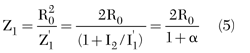
where α= I2/I'1. Because the magnitude of I'1 equals that of I1, the actual load impedance of the carrier amplifier can be modulated as α varies from 0 (|I2|= 0) to 1 (|I2| = |I'1|).

At the mid power level, the peaking amplifier works in the transition region between OFF and ON, where the carrier amplifier has a load modulation from 2R0 to R0. Since the carrier amplifier operates under dynamically varying load impedances, according to the output power level, it is generally biased to a class AB point for enough gain even at a very low power level. It should also show good performance while the load impedance varies from 2R0 to R0.

Figure 6 Operational class variations over the load impedance increase for a fixed quiescent current level.
Even for a fixed quiescent current of IDQ, the operational class of the carrier amplifier can also vary according to the load impedance. If the carrier amplifier is intended to have a class AB bias point for the load impedance R0 at the peak power level, its operation class approaches to a class A as the load impedance is modulated to 2R0 (see Figure 6). In other words, the conduction angle for the load impedance 2R0 is much larger than that for R0.
Compared to a class F amplifier, the class F-1 amplifier has less degradation in PAE at an increased bias condition.9 Hence, it can be easily surmised that the class F-1 amplifier would outperform the class F amplifier at larger load impedance. A two-tone harmonic balance simulation was conducted to verify this hypothesis. The load impedance of the carrier amplifier was swept from 50 Ω (R0) to 100 Ω (2R0). Both the simulated PAE and output power performance of the class F-1 amplifier became better and better than the performance of the class F amplifier at the fixed IMD3 level as the load impedance increased (see Figure 7).

Figure 7 Simulated PAE and output power for the class F and F-1 amplifiers at an IMD3 level of -30 dBc for various load impedances.
Therefore, it can be concluded that the class F-1 amplifier should be selected for the carrier amplifier rather than the class F amplifier in spite of their similar performance at the class B bias condition. In the previous subsection, the class F amplifier was already chosen as the peaking amplifier. The new Doherty amplifier configuration, using class F and class F-1 amplifiers, is shown in Figure 8.

Figure 8 Schematic diagram of the designed Doherty amplifier.
Verification for the New Configuration
To validate the proposed Doherty amplifier configuration, deploying the class F amplifier for the peaking amplifier and the class F-1 amplifier for the carrier amplifier, all four possible configurations for the Doherty amplifier using class F and F-1 amplifiers were compared. They are also compared with the conventional Doherty amplifier using a class AB carrier amplifier and class B peaking amplifier.
The class F, F-1, AB and B amplifiers for the 1.0 GHz band were designed for the simulation using a 4 W LDMOS FET. A two-tone harmonic balance simulation was carried out for each possible configuration after optimizing each to have its best performance by tuning the offset lines and the bias condition of the peaking amplifier. The carrier amplifiers have the same fixed IDQ of 25 mA for all of the configurations, while the peaking amplifiers had optimized bias conditions, which were near the class B point and not significantly different from each other. The simulated results for the five configurations are summarized in Table 2, where the data for the two-tone test was extracted at an IMD3 of -30 dBc.

As expected, the configuration using the class F-1 carrier amplifier and the class F peaking amplifier exhibited the highest output power and PAE at the same time among any other combinations using class F and F-1 amplifiers. The opposite configuration using a class F carrier amplifier and class F-1 peaking amplifier exhibited the worst. This backed up the analyses and descriptions in the previous subsections.
Compared with the conventional class AB and B based Doherty amplifier, the best configuration delivered more output power, as much as 0.76 dB, and better PAE, as much as 6.03 percent points, at an IMD3 of -30 dBc. Benefiting from harmonic tuning and proper selection for the carrier and peaking amplifiers, these amplifiers can further gain approximately a 10 percent higher peak PAE for a one-tone signal input than that of a conventional Doherty amplifier.
Implementation and Experimental Results
Because conventional Doherty amplifiers are generally built with identical cells for both carrier and peaking amplifiers, the phase difference of the transmission coefficient between the carrier and peaking amplifier is not significant and can be easily compensated using a tuned input offset line. However, in this case, the difference in the phase response between the class F-1 carrier and class F peaking amplifiers should be carefully considered since different amplifiers are employed as the carrier and peaking amplifier cells.

Figure 9 Measured phase response of the carrier and peaking amplifiers.
The amplitude modulation to phase modulation (AM to PM) characteristics for the carrier and peaking amplifiers were measured using a network analyzer. Figure 9 shows the measured phase responses of the carrier and peaking amplifiers. As shown, the phase response of the peaking amplifier experienced a huge transition due to a class B bias point while that of the carrier amplifier appeared to be rather flat. The phase difference of about 54.35° was observed around 1 dB gain compression point. It was compensated using an input offset line which was already presented in Figure 8.

Figure 10 Photograph of the implemented Doherty amplifier.
The Doherty amplifier based on class F and F-1 amplifiers was implemented using the same device that was used for the design and simulation. Figure 10 shows a photograph of the implemented Doherty amplifier. The fundamental load impedance of (21 + j19) Ω, extracted from the class AB amplifier design, was applied for both the class F and F-1 amplifiers. The output offset lines were also added at the end of each amplifier, after the matching networks, to have a proper load impedance modulation. The difference of the output offset lines between the carrier and peaking amplifiers was also compensated in the input offset line. The efficiency and linearity of the Doherty amplifier were simultaneously optimized using a bias adjustment especially for the peaking amplifier. The optimum quiescent current (IDQ) for the peaking amplifier was 1.25 mA, which was almost a class B condition. The quiescent current of the carrier amplifier was 25 mA.

Figure 11 Measured performances of the implemented Doherty and balanced amplifiers: (a) IMD3, (b) PAE for a two-tone signal and (c) PAE for a one-tone signal.

Figure 12 Measured performance of the implemented Doherty and balanced amplifiers using a down-link WCDMA signal: (a) ACLR at 2.5 MHz offset and (b) PAE.
The Doherty amplifier was evaluated using the one-tone, two-tone and down-link WCDMA signals. The WCDMA signal has a PAR of 10.5 dB at a complementary cumulative distribution function (CCDF) of 0.01 percent. To see if the load modulation successfully happened, the performance was compared with those of the balanced amplifier with the same amplifier cells. Figure 11 shows the IMD3 and PAE performance for a two-tone excitation at a center frequency of 1 GHz with a tone-spacing of 5 MHz. Compared with a balanced amplifier, improvements in IMD3 of 2.7 dB and PAE of 9.17 percent points were obtained for the Doherty amplifier at an output power of 36 dBm at the same time. Furthermore, a 0.21 dB higher output power and a PAE as high as 50.9 percent were extracted for the Doherty amplifier at an IMD3 level of -30 dBc. The proposed Doherty amplifier presented a peak PAE of 57.4 percent for the one-tone test, as shown also in the figure.
Figure 12 shows the PAE and adjacent channel leakage power ratio (ACLR) performances for the single-carrier down-link WCDMA signal. The proposed Doherty amplifier simultaneously exhibited an improved ACLR by 1.71 dB and a higher PAE by 11.26 percent points at an output power of 34 dBm. More output power, 0.32 dB, and a PAE of 45.2 percent were obtained using the Doherty amplifier at an ACLR of -30 dBc at a 2.5 MHz offset. Table 3 shows a comparison between the measured results in this work with previous works.

Conclusion
To improve efficiency under a critical linearity specification for high-power amplifiers, a Doherty amplifier based on class F and F-1 amplifiers is proposed. In the new Doherty configuration, class F-1 and F amplifiers are used as the carrier and peaking amplifiers, respectively. To determine the Doherty amplifier configuration, the properties of the class F and F-1 amplifiers were comprehensively investigated and compared with each other.
The class F amplifier turned out to be best suited for the peaking amplifier because of the large gain expansion characteristics for operation at a low bias point. On the other hand, the class F-1 amplifier was verified to have better performance at higher load impedance, using load line analysis and simulation, which was why it was selected for the carrier amplifier.
The high-efficiency class F and F-1 amplifiers were designed and implemented for the 1 GHz band. Their performance was optimized to have the highest possible PAE under a given linearity specification as an IMD3 of -30 dBc. The simulated and measured performances were compared to the simulated conventional class AB amplifier. Using the designed class F, F-1, AB and B amplifiers, various configurations for the Doherty amplifier were synthesized and compared to each other using harmonic balance simulations. As expected, the proposed Doherty configuration significantly outperformed among all the others.
For experimental verification, the proposed Doherty amplifier was implemented as designed using Freescale’s MRF281S, a 4 W-PEP LDMOS FET. The measured results include significantly improved performance for the Doherty operation compared to those for the balanced operation. A PAE of 50.9 percent was obtained for the two-tone test at an IMD3 of -30 dBc with a 5 MHz tone spacing. A PAE of 45.2 percent was achieved for the down-link WCDMA signal at an ACLR of -30 dBc at a 2.5 MHz offset using the proposed Doherty amplifier. Both are showing state-of-the-art efficiency performances for the given linearity levels among the previously reported Doherty amplifiers.
References
1. Y. Yang, J. Cha, B. Shin and B. Kim, “A Fully Matched N-way Doherty Amplifier with Optimized Linearity,” IEEE Transactions on Microwave Theory and Techniques, Vol. 51, No. 3, March 2003, pp. 986-993.
2. G. Ahn, M. Kim, H. Park, S. Jung, J. Van, H. Cho, S. Kwon, J. Jeong, K. Lim, J. Kim, S. Song, C. Park and Y. Yang, “Design of a High-efficiency and High-power Inverted Doherty Amplifier,” IEEE Transactions on Microwave Theory and Techniques, Vol. 55, No. 6, June 2007, pp. 1105-1111.
3. H. Park, J. Van, S. Jung, M. Kim, H. Cho, S. Kwon, J. Jeong, K. Lim, C. Park and Y. Yang, “A New Compact Load Network for Doherty Amplifiers Using an Imperfect Quarter-wave Line,” IEEE Transactions on Microwave Theory and Techniques, Vol. 55, No. 11, November 2007, pp. 2313-2319.
4. J. Cha, J. Kim, B. Kim, J. Lee and S. Kim, “Highly Efficient Power Amplifier for CDMA Base Stations Using Doherty Configuration,” 2004 IEEE MTT-S International Microwave Symposium Digest, pp. 533-536.
5. K. Cho, I. Hwang, W. Kim, J. Kim and S.P. Stapleton, “Linearity Optimization of a High Power Doherty Amplifier,” 2005 IEEE MTT-S International Microwave Symposium Digest, pp. 1387-1390.
6. Y. Zhao, A.G. Metzger, P.J. Zampardi, M. Iwamoto and P.M. Asbeck, “Linearity Improvement of HBT-based Doherty Power Amplifiers Based on a Simple Analytical Model,” IEEE Transactions on Microwave Theory and Techniques, Vol. 54, No. 12, December 2006, pp. 4479-4488.
7. H. Park, G. Ahn, S. Jung, C. Park, W. Nah, B. Kim and Y. Yang, “High Efficiency Class-F Amplifier Design in the Presence of Internal Parasitic Components of Transistors,” Proceedings of the 36th European Microwave Conference, September 2006, pp. 184-187.
8. S. Gao, P. Butterworth, S. Ooi and A. Sambell, “High Efficiency Power Amplifier Design Including Input Harmonic Termination,” IEEE Microwave and Wireless Components Letters, Vol. 16, No. 2, February 2005, pp. 81-83.
9. S. Goto, T. Kunii, A. Ohta, A. Inoue, Y. Hosokawa, R. Hattori and Y. Mitsui, “Effect of Bias Condition and Input Harmonic Termination on High Efficiency Inverse Class-F Amplifiers,” Proceeding of the 31st European Microwave Conference, October 2001, pp. 1-4.
10. A. Ohta, A. Inoue, S. Goto, K. Ueda, T. Ishikawa and Y. Matsuda, “Intermodulation Distortion Analysis of Class-F and Inverse Class-F HBT Amplifiers,” IEEE Transactions on Microwave Theory and Techniques, Vol. 53, No. 6, June 2005, pp. 2121-2128.
11. S. Goto, T. Kunii, A. Inoue, K. Izawa, T. Ishikawa and Y. Matsuda, “Efficiency Enhancement of Doherty Amplifier with Combination of Class-F and Inverse Class-F Schemes for S-band Base Station Application,” 2004 IEEE MTT-S International Microwave Symposium Digest, pp. 839-842.
12. J. Kim, J. Moon, Y.Y. Woo, S. Hong, I. Kim, J. Kim and B. Kim, “Analysis of a Fully Matched Saturated Doherty Amplifier with Excellent Efficiency,” IEEE Transactions on Microwave Theory and Techniques, Vol. 56, No. 2, February 2008, pp. 328-338.