
In this article a temperature dependent equivalent circuit of a forward-biased PIN diode is discussed. Using this equivalent circuit, the temperature behavior of a PIN diode attenuator circuit is analyzed and test results are presented. A novel control circuit is also offered for temperature invariant variable attenuation over a very wide range of temperature. This proposed circuit uses no separate temperature sensor or compensating mechanism, but responds directly to the junction temperature of the PIN diode. The junction temperature of the PIN diode modifies the diode current in such a way that its RF resistance remains invariant over the temperature range. This prevents any errors caused by temperature gradients, or by self-heating of the diodes due to high RF levels.
PIN diodes have been widely used in various microwave and RF applications wherever an electronically variable RF resistance is required, such as in variable attenuators, phase shifters, linearizers, variable gain amplifiers, electronically steered array antennas, etc. In general, a PIN diode’s RF resistance is controlled by adjusting the bias current, since it is known that a PIN diode works as a current-controlled device. Under constant current bias conditions, however, the RF resistance of commercially available PIN diodes varies with temperature, which results in the RF attenuation also varying with temperature.
Several vendors have developed digital as well as analog compensation circuits to achieve the required attenuation accuracy over the operating temperature range. However, they have the disadvantage of a relatively complex circuit with higher part-count and size, and lower reliability.
A temperature dependent, forward-biased PIN diode equivalent circuit is presented. The analysis of this circuit leads to a variable attenuator that offers a temperature invariant attenuation without sacrificing the simplicity and reliability of the circuit. This extremely simple topology exploits an interesting feature of the PIN diode to achieve good temperature stability and ease of adjustment.
Diode model
Figure 1 shows the equivalent circuit of a forward-biased PIN diode. Here, RJ is the junction resistance of the diode obtained from the well known I-V relationship given by1

where
Eb = band gap potential of the semiconductor in volts
? = ideality factor of the diode
q = electron charge
k = Boltzman’s constant
n = temperature exponent
A = constant, independent on the temperature T
RI is the effective high frequency resistance of the diode which is related to the DC bias current2 and the operating temperature,3,4 by the relation

where
CI = equivalent I layer capacitance
RS = series resistance
LP = package inductance
CP = package capacitance
Lh = high value inductor included to separate the DC and RF circuit components
Ch = high value capacitor included to separate the DC and RF circuit components
Test Results
Figure 2 shows the MIC layout and assembly drawing of a C-band (3.4 to 4.0 GHz) attenuator circuit used to prove the temperature dependent PIN diode model and the design principles presented here. D1 and D2 are the beam lead PIN diodes (MPND-4005) mounted in a 3 dB Lange coupler. The HP EEsof’s Series-IV Libra simulator was used to simulate and analyze the circuit.

Fig. 1 Equivalent circuit of a PIN diode.

Fig. 2 MIC layout and assembly drawing of a PIN diode attenuator.
Figure 3 shows the measured and simulated I–V characteristic of the PIN diode at three different diode temperatures. The fitting parameters of Equation 1 are n = 2, Eb = 2.12 V and ? = 2.1. The voltage and current of the diode are measured by applying a pulsed voltage to avoid self-heating of the diode.
Figure 4 shows the measured and simulated attenuation versus DC bias current for the diode at three different temperatures at a frequency of 3.7 GHz. The fitting parameters of Equation 2 are m = 1.15, p = 0.88, Rs = 4.5 ?, CI = 0.02 pF and Lp = Cp = ?.
Figure 5 shows the measured and simulated attenuation performance over the frequency band of 3.4 to 4.0 GHz at three different constant bias current (0.18, 0.38, 0.68 mA) settings at three different operating temperatures (–10°, +22°, +60°C).
It also shows how the attenuation varies when the PIN diode is biased by a constant current. An attenuation setting of 20 dB at –10°C decreases to 15 dB at a temperature of 60°C when the bias current of each diode is kept constant at 0.68 mA.
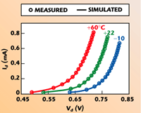
Fig. 3 I-V characterisitcs of a PIN diode.

Fig. 4 Attenuation vs. bias current.

Fig. 5 Attenuation vs. frequency for different currents and temperatures.
All the plots have shown good agreement between simulated and measured results, which proves the validity and accuracy of the temperature dependent PIN diode model under forward bias condition.
A simple bias circuit for the PIN diode attenuator consists of a voltage source V and a series resistor R, as shown in Figure 6. This circuit has been simulated and analyzed using the described equivalent circuit of the PIN diode to see the effect of the bias circuit on attenuation over the temperature range. These simulated results are shown in Figure 7. It shows very interesting characteristics of the attenuator:
• The attenuation decreases with increasing temperature when PIN diodes are biased by a very high voltage source and high value of bias resistor (equivalent to constant current source bias).
• The attenuation increases with an increase of the temperature when PIN diodes are biased by a low voltage and low value of bias resistor.
• The attenuation remains invariant with temperature when the diodes are biased with a voltage source of 1.19 V.

The measured results of the attenuator when the diodes are biased with a voltage source of 1.19 V are shown in Table 1. The different attenuation settings, from 0 to 20 dB in steps of 5 dB, are achieved by setting different values of the resistor R. This table shows that the peak-to-peak variation of all the step attenuations is less than 0.5 dB over the temperature range of –10° to +60°C and over the entire 3.4 to 4.0 GHz frequency band.
Thus, from the above discussions, it can be concluded that for conventional constant current bias conditions, the attenuation of a PIN diode attenuator changes with temperature. When the PIN diode is biased by an optimum voltage source of 1.19 V (for a MPND4005 diode), however, the current through the diode is controlled in such a way that the RF resistance of the diode remains constant over the temperature range.
Theoretical explanations
To achieve a temperature invariant attenuation of the PIN diode attenuator, the bias network must meet the current required to achieve a constant RF resistance, RIO, of the PIN diode, over the temperature range. Therefore, by combining Equations 1 and 2 and setting RI = RIO,

where Vd(T) is given by

This parametric equation is the equation of the ideal bias-point locus that will satisfy RI = RIO across the temperature range. This locus is called the equi-resistance curve for the required RF resistance RIO.
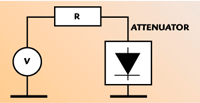
Fig. 6 Simple bias circuit of an attenuator.
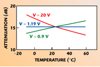
Fig. 7 Attenuator vs. temperature for different bias sources.
Figure 8 shows the plot of Equation 3 for the MPND-4005 diode over the temperature range of –260° to + 300°C for an RF resistance RIO = 70 ?. The constant resistance curve is highly linear within the temperature range of interest. Thus, the load line of the simple bias circuit can be adjusted to coincide with this curve within the temperature range of interest and will then maintain the desired RF resistance. The voltage of the bias network will be the voltage intercept of the bias line and resistance will be the reciprocal of the slope of bias line.
Fig. 8 Equi-resistance curve and load line for the MPND-4005 diode.
Combining Equations 3 and 4 and eliminating the parameter T, another form of the equation of the equi-resistance curve can be written as

The equation of the tangent to this equi-resistance curve at the diode voltage Vx and corresponding current Ix at temperature Tx is given by

Taking this tangent to be the optimum load line, its voltage intercept is

This optimum voltage Vopt will be the open circuit voltage of the bias network.
Figure 9 shows the variation of Vopt for different attenuation (5, 10, 15, 20 dB) requirements (corresponding to different Vx) at three different temperatures (–10°, + 25°, +60°C). It is clear that Vopt is nearly invariant about the value of 1.19 V for different attenuations and temperatures. Theoretically it can be shown that for all practical values of diode parameters n, m and p the value of Vopt will be invariant over a wide range of temperature for different values of attenuation.

Fig. 9 Variation of Vopt with temperature and attention
Control Circuit for Variable Attenuator
From the above theoretical discussion and test results it is clear that the equi-resistance curves of the PIN diode become straight lines over a very wide range of temperature and the optimum load lines for different attenuation settings intersect the voltage axis at nearly the same point.

Fig. 10 Temperature invariant variable PIN diode attenuator circuit.
Therefore, a control circuit for temperature invariant attenuation can consist of a voltage source and a series resistor. Figure 10 shows a proposed simple variable attenuator circuit which will provide a temperature invariant attenuation. Here, Vopt is the optimum open-circuit voltage source of value given by Equation 7. Different attenuation settings will be achieved by switching or varying the value of the resistor R.
This attenuator circuit has been realized with different types of beam lead PIN diodes available, e.g. Metalics’ MPND-4005, Hewlett Packard’s HPND-4005 and Infinion’s BXY-44K. It has been verified that this proposed circuit is applicable for all the diodes.
Conclusion
It can be concluded that the described temperature dependent, forward-biased PIN diode model is accurate enough to analyze the temperature behavior of the PIN diode attenuator circuit. Using this temperature dependent PIN diode model, a simple bias circuit is proposed that will provide a temperature invariant attenuation. The proposed circuit uses no separate temperature sensor or compensating mechanism, but responds directly to the junction temperature of the diodes. The junction temperature of the PIN diode modifies the diode current in such a way that the RF resistance of the diode remains invariant over the temperature. This prevents any errors caused by temperature gradients, or by self-heating of the diodes due to high RF levels. It is also verified that this approach can be used for a wide range of available diodes.
References
1. J. Millman and C.C. Halkias, Integrated Electronics, McGraw-Hill International Editions, 1988.
2. Hewlett-Packard Application Note No. 922.
3. R.H. Caverly and G. Hiller, “The Temperature Dependence of PIN Diode Attenuators,” IEEE International Microwave Symposium Digest, 1993, pp. 553–556.
4. R.H. Caverly and G. Hiller, “Temperature Effect on PIN Diode Forward Bias Resistance,” Solid State Electronics, Vol. 38, No. 11, 1995, pp. 1879–1885.