
This article describes the architecture of a power amplifier module for polar-modulated schemes. Polar-modulated power amplifiers use polar coordinates' representation of a signal-vector (vs. the traditional Cartesian I-Q representation used in the W-CDMA modulation scheme, for example). In this scheme, the recombination of coordinates is done at the output of the power amplifier. It is employed to make use of highly nonlinear (that is, very efficient) RF power amplifiers. However, the recombination of polar coordinates is essentially a nonlinear process. It means that the amplifier should stay nonlinear (with preferably unchanged level of nonlinearity) all the time and under all conditions.
In this article, a theory of a polar modulation is given. Based on it, the required degree of a power amplifier's nonlinearity is figured out. It is demonstrated that nonlinearity, while being a necessity, cannot become too large either. A straightforward method of keeping up the allowed nonlinearity window is shown and its shortcomings are pointed out. Finally, improvements are introduced and explained in detail. The resulting architecture allows a correct recombination of polar coordinates under any conditions of power amplifier operation.
Polar Modulation
The polar modulation concept is based on the fact that pure phase modulation does not create intermodulation products (sidelobes). The sidelobes are distorting a spectral mask. They are the reason for employing highly linear amplifiers. In case of phase-modulated signals, though, one can use very nonlinear (that is, very efficient) amplifiers. It will be shown that polar modulation actually requires a very nonlinear amplifier for proper operation.
Modern digital communications are characterized by their constellation diagrams, created by the positions of a signal-vector. Each modulation scheme defines a constellation diagram (QPSK, 3π/4 DQPSK, 64QAM, etc.), the transmitter produces it, and the receiver looks for signals in predetermined positions of the diagram. Traditionally, the positions of a signal-vector are described by Cartesian coordinates (Real and Imaginary, that is I-Q); however, the same positions can be exactly described by polar coordinates (amplitude and phase or magnitude and angle). The polar presentation allows at least the phase portion of a signal-vector representation to be amplified by very efficient amplifiers. The magnitude portion of a signal-vector is just a discrete DC variation, that is, requires no sophisticated amplifiers.
A concept of a polar-modulation scheme is explained in detail by F. Ditore1 and its block diagram is given in Figure 1. Usually, instead of the combination of a magnitude amplifier and a combiner, the signal from an envelope detector is applied directly to the collector of the output stage of a phase amplifier. It simplifies the block diagram, but creates its own challenges.
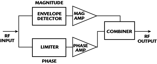
Figure 1 Block diagram of a concept of polar modulation.
Requirements to Polar-Modulated Power Amplifiers
The separation of the RF input signal into magnitude and phase is essentially a nonlinear process. As follows from the figure, it includes two highly nonlinear components: an envelope detector and a limiter. This immediately suggests the need for a nonlinear recombination. Since, in polar modulation, the recombination is done at the power amplifier itself, it has to be nonlinear. The degree of nonlinearity is determined from the required dynamic range.
The dynamic range of the EDGE waveform (the standard where polar modulation is most commonly used) is approximately 17 dB, as follows from the Agilent ADS time domain presentation of undistorted EDGE source, shown in Figure 2. This dynamic range has to be reproduced by the variation of magnitude portion of a polar-modulated signal (since the phase portion produces a constant envelope). According to the commonly accepted architecture, the signal from an envelope detector (representing the magnitude of a signal-vector) is applied directly to the collector of an output stage of the amplifier. The only way to replicate magnitude variations is to use a nonlinear amplifier, since an amplifier in a linear mode of operation is DC supply independent. The amplifier has to be nonlinear enough to reproduce 17 dB of magnitude variation.

Figure 2 Time domain presentation of an undistorted EDGE source.
The degree of nonlinearity, though, depends on the input RF power and the DC bias voltage. The higher the input power or/and the lower the DC bias, the more nonlinear the amplifier. To estimate the degree of a power amplifier's nonlinearity needed to produce 17 dB of dynamic range, consider the following example:
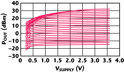
Figure 3 Dependence of the output power on the DC voltage of a typical BJT transistor.
A typical set of graphs of output power vs. DC bias for a 1 W BJT transistor is shown in Figure 3, where the input power is varied from -20 to +20 dBm. From the figure, it follows that, at high input power levels, 17 dB of magnitude variation is achieved with DC variation from 3 down to 0.2 V. It is also interesting to note that the amplifier becomes unacceptably linear when the input RF power level drops by just a few dB. However, the degree of amplifier nonlinearity has its limitations. It cannot be too large. The reason for that is in the accuracy of polar coordinates' recombination at the output of the power amplifier. The relationship between polar coordinates at its output should be the same as at the input. This relationship is expressed as AM-AM and AM-PM characteristics. They show dependence of the output magnitude and phase on the input magnitude. Ideally, there should be no phase variation and a straight line coming through the origin in magnitude variation, as demonstrated in Figure 4.
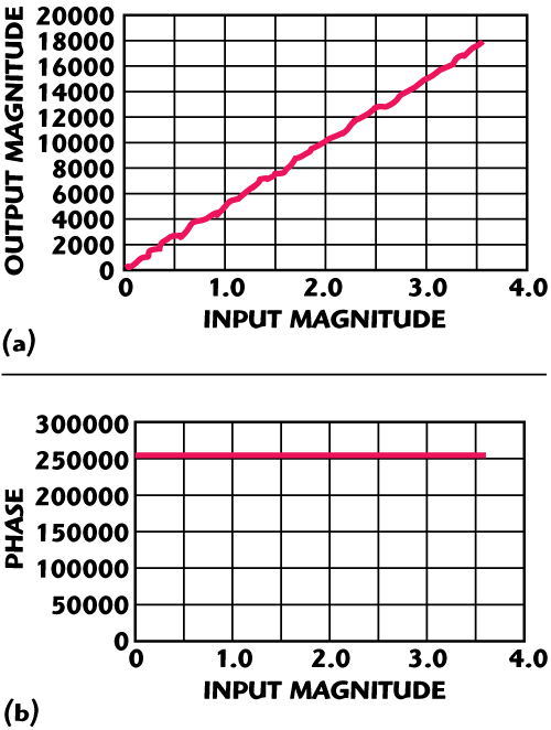
Figure 4 Ideal relationship between input and output variations magnitude (a) and phase (b).
Keeping up the acceptable level of recombination accuracy is challenging. The reason for the challenge is in the output parasitic capacitance of BJT transistors (Miller capacitance).2 It is a variable capacitance, the value of which depends on the applied collector voltage. The problem with that capacitance is that it rotates the phase of the input phase signal, and the rotation depends on the capacitance value. The effect is most pronounced at low collector voltages (up to 0.3 to 0.4 V) and is observed in the nonlinear behavior of AM-AM and AM-PM characteristics, causing their misalignment. A typical set of AM-AM and AM-PM graphs is given in Figure 5, where Vramp is the voltage applied to the collector of the output transistor. From the figure, it follows that a somewhat linear behavior of AM-AM and AM-PM characteristics happens only when Vramp is above 0.3 V. The amplifier is still nonlinear enough when collector voltages vary from 3 down to 0.3 V (see Figure 3); however, this example shows how sensitive the nonlinearity setting is in polar-modulated amplifiers.
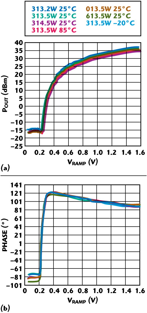
Figure 5 Typical AM-AM (a) and AM-PM (b) performance of a polar-modulated amplifier at 900 MHz.
It is important to make the amplifier nonlinear enough - to ensure the required dynamic range of coordinates' recombination, and, at the same time, to be not very linear - to keep the acceptable accuracy of the recombination. A straightforward solution of these contradicting requirements is to fix the input RF power at high level (approximately 20 dB in the example), and to make the DC supply voltage higher than a threshold level (0.3 V in the same example). The variation of RF power, requested by the base station, is done at the output of the amplifier.
Shortcomings of Straightforward Implementation
The straightforward implementation of a polar modulated amplifier works in principle; its approach is documented.3 Its block diagram is shown in Figure 6. It is almost the same as the block diagram of the concept of a polar-modulation scheme (see Figure 1), only with the addition of a "smart" attenuator (MA) and a "smart" DC bias (LF-AMP). However, one should avoid placing components with RF loss at the amplifiers' output. The specific reasons for NOT placing an attenuator to the output of a polar-modulated amplifier include:
- It is an inefficient mode of operation. Every 3 dB reduction of RF power level by the output attenuator leads to halve the initial efficiency of the power amplifier. For example, if the power amplifier is biased for 60 percent efficiency at 30 dBm of output power and the base station requests 27 dBm of output power, then the module would operate with only 30 percent efficiency.
- The amplifier is becoming "unprotected" at its input. If for any reason an input RF power level is reduced, the PA would slip out of its nonlinear mode of operation (which means that it would no longer recombine magnitude and phase correctly).
- The output attenuator has to operate at high powers, so it would require PIN diode implementation. It is also expensive, since PIN diodes could not be made in the same IC die as the power amplifier itself.

Figure 6 Block diagram of a polar-modulated amplifier meeting the nonlinearity requirements.
Power Amplifier Module for Polar Modulation
The recombination of polar coordinates has to be done on a nonlinear component. It would be nice if that component was an amplifier itself, but any nonlinear enough components would do the job. Instead of adding a "smart" attenuator to the output of the amplifier, add a "smart" multiplier to its input. The job of that "smart" multiplier would be to recombine coordinates when the amplifier itself is in a linear mode (that is, when the RF power level is too low or DC bias is too high) and to be transparent when the amplifier is nonlinear enough. It leads to the block diagram of a polar-modulated power amplifier module shown in Figure 7.

Figure 7 Block diagram of a polar-modulated power amplifier module.
A RF signal from a limiter (phase) is applied to Switch 1. The function of this switch is to send an input signal either directly to the input of the power amplifier (when it operates in nonlinear mode) or to the RF input of a low-power multiplier (when the amplifier is linear). A DC variable signal from the envelope detector (magnitude) is applied to the LO input of a low-power multiplier and simultaneously to Switch 2. The function of Switch 2 is to apply the magnitude signal either to the collector of the amplifier (when it operates in nonlinear mode), or to switch its collector to the battery with fixed voltage, labeled "DC power Supply" (when the amplifier is linear). Switch 1 has a neutral position "P3", which is used during the operation of Switch 2 (to ensure that the switching between the fixed battery and magnitude signal is done when no RF input is present). This architecture affords an efficient mode of an amplifier's operation (since there is a possibility to provide a nonlinear bias to the amplifier for any given level of RF input power using a look-up table, for example); it is going to work at any conditions of RF input power even if the amplifier is linear at those conditions. This solution can be implemented in the same die as an amplifier itself, which, for all practical terms, does not increase the cost of solution.
Conclusion
In this article, an optimum architecture of a power amplifier module for polar-modulated schemes was derived. In the process of its derivation, a theory of polar modulation was given. It was made clear that in order to properly recombine polar coordinates, the power amplifier has to be nonlinear. It was also emphasized that the degree of nonlinearity has its limits, determined by the accuracy of the polar coordinates' recombination, and that limitation is fundamental (due to Miller capacitance, intrinsic to the die). It was pointed out that the most logical method of keeping up a predetermined level of nonlinearity is not efficient and expensive. Finally, a module architecture, offering a more efficient operation and less expensive implementation, was introduced. The offered solution works for any mode of power amplifier operation, allowing integrators to concentrate on the optimum mode rather than to worry about operability of the module.
References
1. F. Ditore, "Polar Modulation Ups Efficiency in Mobile PA Designs," CommsDesign, September 4, 2003.
2. P. Reynaert and M.S.J. Steyaert, "A 1.75 GHz Polar Modulated CMOS RF Power Amplifier for GSM-EDGE," IEEE Journal of Solid-State Circuits, Vol. 40, No. 12, December 2005, pp. 2598-2608.
3. A. De Graauw and L. Van Den Oever, "Amplifier Architecture for Polar Modulation," Patent Publication # WO 2008/032264 A2.