
A phase-locked loop (PLL) is a popular method used in frequency synthesizers for most communication systems.10 The block diagram of a common PLL synthesizer is shown in Figure 1 and includes a charge pump phase detector (PD), a temperature-compensated crystal oscillator (TCXO), a voltage-controlled oscillator (VCO), an R divider and an N divider. Kv is the VCO gain constant (MHz/V), Kp is the PD gain constant (mA/rad) and Z(s) represents the loop filter transfer function. The R divider divides down the TCXO frequency to form a channel and the N divider divides down the VCO frequency. The PD compares the two divided-down signals and generates current pulses proportional to the phase difference. The PD’s output current pulses are filtered by the loop filter and a slow varying voltage tunes the VCO frequency to ultimately drive the PD’s average output to zero.
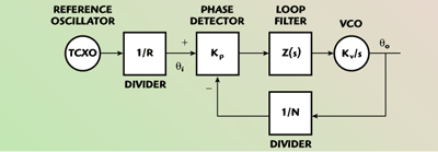
Fig. 1 Block diagram of a PPL synthesizer.
A PLL frequency synthesizer can be simply frequency modulated by injecting the modulation signal Vm into the tuning input of the VCO. However, the modulation response for Vm has a high pass characteristic as
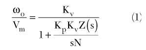
From Equation 1, it can be found that for modulation rates greater than the PLL loop bandwidth the VCO can be modulated successfully. However, for rates less than the loop bandwidth, there is no modulated output. Narrowing the loop bandwidth will result in a longer lock time that the system may not tolerate. This article reviews some of the techniques used to overcome this problem and introduces a practical low cost modulation circuit.

Fig. 2 Frequency modulation methods in PLLsynthesizers; (a) FM PLL using a phrase modulator, (b) FP PLL using a VCXO and (c) FM PLL using compensation of the amount of feedback.
Frequency modulation using a PLL
Figure 2 shows methods used by others to circumvent this problem. In the method using a phase modulator,2 the signal Vm1 injected into the VCO generates the high pass modulated signal given in Equation 1 and the Vm2 injected into the phase modulator through the integrator yields the low pass modulated signal as
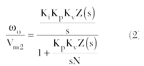
If Vm= V m1+ Vm2(the modulation signal Vmis split into two paths as Vm1and Vm2) and Ki= Kv/N, the VCO output for Vmis the sum of Equations 1 and 2 and results in a flat peak frequency deviation ?f, independent of the modulation rates. In the method using a VCXO,3for a low frequency modulation, Vm2, split from Vm, is injected to the voltage-controlled crystal oscillator (VCXO) instead of the TCXO. A flat ?f, independent of the modulation rates, can be obtained if
Although the previous two-point modulation methods (one injection point is the VCO tuning input for high pass characteristic modulation and the other is the potential point providing a low pass characteristic modulation) provide a modulation response extending down to DC, they require specific highly priced components such as a phase modulator and VCXO.

Fig. 3 Compensation circuit for the amount of feedback.
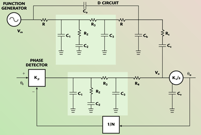
Fig. 4 FM PLL with a third-order loop filter.
The block diagram of an FM PLL using compensation of the amount of feedback is also shown. The amount of feedback in the denominator of Equation 1 is compensated by the modulation block D. For complete compensation, the modulation block should have a transfer function given by
By multiplying Equations 1 and 2, the VCO may then generate an FM modulated signal with a desired peak frequency deviation ?f.
The modulation block can be implemented by various circuits for the given PLL loop filter. For the second-order charge pump loop filter Z(s) of R1, C1 and C2, Rosemarin4 has suggested the circuit shown in Figure 3.
In this circuit, the output voltage across Cb will be developed by two currents, iR and iC. Assuming that R is large enough (R/2 >>?Z(s)?) to act as a current source and using superposition, Vo can then be approximately written as
From R/2>>?Z(s)?, the values of R can be consequently determined by
where
fmin = minimum frequency of the modulation signal
Comparing Equation 3 with Equation 4, Ca should satisfy the relation
Finally, Cb can be determined to give the desired ?f as
Although the above circuit is designed for a one-port, second-order charge pump loop filter, the circuit can be applied successfully for a two-port higher order loop filter frequently employed for the sufficient suppression of spurious. However, the circuit is easily influenced by the load (load impedance is open in the derivation). As a result, the proper separation or the compensation of the loading effect is required in the application.
Figure 4 shows the proposed overall FM PLL synthesizer including the modulation block determined as in the previous case. Rc and Cc are inserted for the compensation of the PLL loop filter loading. The Cc capacitor also plays a role in blocking the leakage of the DC voltage at the VCO input to the modulation block. The third-order loop filter is chosen for the sufficient attenuation of the spurious. R4 with the VCO input parasitic capacitance Cv = 550 pF may increase the order of the loop filter; however, its time constant is selected far above the channel frequency to yield a negligible effect on the loop filter. R4 is inserted to prevent the direct loading of Cv to the designed C3.
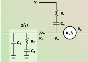
Fig. 5 Approximated circuit of theFM PLL with a third-order loop filter.
The FM PLL synthesizer has a center frequency of 164 MHz, a channel spacing of 12.5 kHz and the desired peak frequency deviation ?f of 2.4 kHz. The VCO and PD gain constants are Kv = 17 MHz/V and Kp = 5 mA/rad, respectively. The third-order loop filter is calculated by following Baberjee’s method5 with a phase margin of 45° and a loop bandwidth of 1 kHz, taking the lock time specification into consideration. The calculated element values are C1 = 68nF, R2 = 1.2 kW, C2 = 680 nF, R3 = 33 k?, C4 = 560 pF and R4 = 1.8 k?.
The element values of the modulation block are Ca = 3.75 pF, Cb = 6.8 nF and R = 200 k?.
The computed transfer function of the modulation block is actually affected by the connected loop filter. In order to determine RC and CC, an approximated FM circuit is drawn in Figure 5, assuming modulation rates lower than the channel frequency. The output of the modulation block is denoted by Vi. The transfer function then becomes

The second-order loop filter impedance Z(s) can be approximated as the parallel connection of C1 and C2 at a low frequency. In that case, Equation 8 becomes frequency independent of RC and CC if they are selected to satisfy the relation
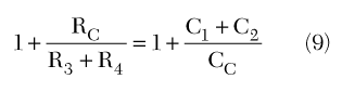
The modulation block output is then scaled down by Equation 8 and transferred to the VCO without distorting its frequency response. However, Equation 8 actually shows weak frequency dependence to some degree. To get the optimum Rc and Cc from the many possible choices given by Equation 9, the circuit in Figure 4 was simulated and tuned using ADS for a flat peak frequency deviation. The best performance is obtained at Cc = 680 nF and Rc = 34.8 k?.
To investigate the loading effect, the higher order loop filter elements (R3, C3 and R4) and the coupling circuit (R4 and Cc) are removed. The values of the remaining second-order loop filter are slightly adjusted for the phase margin of 45° and the loop bandwidth of 1 kHz. The modulation block is also tuned again according to the second-order loop filter change. The modulation signal, with a peak-to-peak voltage of 1 V, is applied through the corresponding second-order modulation circuit. Figure 6 shows the spectra of the second-order FM PLL synthesizer for a modulation signal of 4.8 kHz (modulation index ? = 0.5) and of 400 Hz (? = 6).
At 4.8 kHz, the spurious is found at the channel frequency of 12.5 kHz, resulting from an insufficient attenuation. For 400 Hz, the un-suppressed spurious of 12.5 kHz grows bigger and is also modulated. It should be noted that ?f is decreased. The modulated spectrum of the desired ?f, by Carson’s rule, has a 99 percent BW of 5.6 kHz (BW~(?f + fm) = 2(2.4 + 0.4) = 5.6 kHz.6 But the estimated BW from the modulated spectrum is approximately 4.8 kHz < 5.6 kHz. The decrease of ?f at a low modulation frequency occurs because the effective Cb is increased by the loading of the parallel connection of C1 and C2, which results in the decrease of ?f according to Equation 7.
Figure 7 shows the measured results of the third-order FM PLL circuit. Comparing these results with the last case, the spurious is suppressed sufficiently and does not show in the spectrum. The bandwidth of 5.6 kHz for the desired peak frequency deviation is estimated in the spectrum.

Fig. 6 Second-order FM PLL measurements of the (a) modulated spectrum for 4.8 kHz and (b) modulated spectrum for 400 Hz at f0 = 164 MHz.

Fig. 7 Third-order FM PLL measurements of a (a) modulated spectrum for 4.8 kHz and (b) modulated spectrum for 400 Hz at f0 = 164 MHz.
Novel ?f measurement with a spectrum analyzer
The FM modulated carrier xc(t) by a sinusoidal signal of ?m = 2?fm can be expressed as
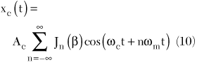
Here, Jn(?) represents an n-th order Bessel function of the first kind. Based on Equation 10, the modulation index (?) can be measured with a spectrum analyzer by three known methods. The first method is to change the modulation rate and to find the rate which yields the first null of the carrier amplitude Jo(?). From this, the value of ?f can be found using the modulation rate and the known first zero of Jo(?). However, for the method of the carrier zeros, the modulation index should be independent of the modulation rate. The method of using the 99 percent power bandwidth is useful to estimate ?f for a wide band FM signal as shown in the previous section. It is not adequate, however, to determine the precise value of ?f. In order to measure the ?f for the modulation rate change, a useful method is based on the recurrence formulas for Bessel function as7
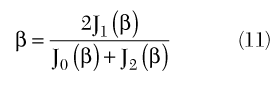
The application of Equation 11 is successful for narrowband FM, considering that the three tones in Equation 10 are dominant. However, the error in the measurement by three tones becomes critical in the determination of the modulation index, especially in wideband FM, although Equation 11 is an exact one. To show this, the ratio bm,2/? is plotted in Figure 8 assuming a random measurement error of 0.1 dB of the spectrum analyzer 8564E. The ?m,2 represents the maximum and minimum of the measured ? determined by Equation 11 with the random measurement error of the spectrum analyzer. The error becomes extremely large near the zeroes of J1(?) because both the denominator and nominator in Equation 11 approach zero simultaneously.

Fig. 8 The calculated ?m,n/? with the spectrum
analyzer error (the subscript n represents the number of tones used in calculation).

Fig. 9 Comparison of the simulated and measured ?f for the proposed FM PLL synthesizer.
To reduce the errors, Equation 11 is modified to contain a large number of tones in the determination of the modulation index. Extending the recurrence formulas up to n+1 tones,

Summing up the left and the right sides of Equation 12, ? can be written as
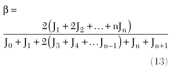
The ?m,30, that is the modulation index determined by Equation 13 using 30 tone measurements, is also plotted and shows an almost flat error and does not show the error peaks compared to ?m,2. From these results, the number of the measured tones is increased according to ? for the proposed FM PLL measurement.
Figure 9 shows the simulated and measured ?f with the suggested method for the proposed FM modulator for the different modulation rates. The results show that a flat frequency deviation, down to 200 Hz, is obtained and shows good agreement with the design. Below 200 Hz, the frequency of the function generator used as the modulation source is unstable, and reliable measurements cannot be obtained.
Conclusion
In this article, a low cost and practical FM PLL synthesizer circuit for a flat peak frequency deviation is suggested based on the amount of feedback compensation. The modulation rate can be extended down to below the PLL loop bandwidth. Rosemarin’s amount of feedback compensation circuit is modified to include a two-port loop filter and consequently suppress the spurious sufficiently. The influence of the loop filter deteriorates the modulation circuit and the interaction should also be compensated. An approximate compensation of the influence is suggested. The possible error in the modulation index measurement is reduced by including a sufficient number of tones. With the suggested measurement, it can be successfully verified that the designed circuit has the expected frequency deviation.
Acknowledgment
This work has been supported by the MINT (Millimeter-wave INnovation Technology) Research Center of KOSEF.
References
1. L. Rohde, Microwave and Wireless Synthesizers, Wiley-Interscience, Somerset, NJ, 1997, pp. 1–78.
2. S. Grimmett, “Frequency Modulation in a Phase-lock Loop by Control of the Phase Inside the Loop,” RF Design, June 1991, pp. 31–38.
3. R. Hunter and F. Kostedt, “Using Tow-point Modulation to Reduce Synthesizer Problems When Designing DC-coupled GMSK Modulation,” MX-COM, 2000.
4. D. Rosemarin, “Wide Bandwidth Frequency Modulation of Phase-lock Loops,” RF Design, February 2000.
5. D. Baberjee, PLL Performance, Simulation and Design, National Semiconductor, 2001, pp. 13–21 or 77–104.
6. M.S. Roden, Analog and Digital Communication Systems, Prentice-Hall, Upper Saddle River, NJ, 1996, pp. 272–315.
7. “Spectrum Analysis Amplitude and Frequency Modulation,” Application Note 150-1, Agilent Technologies.