
Multifunction modules are built from many simpler building blocks. Each block can be in the form of an MMIC device, a discrete component or a hybrid device. These blocks are assembled next to each other and connected by transition lines. There are several disciplines for the assembly process. The most widely used is the open-carrier approach. Each block is assembled on a separate metal carrier. An example, an MIC assembly, is shown in Figure 1. Various assembly techniques are used for each block, such as soldering at various temperatures and epoxy attachment. The assembled block is then tested and sometimes tuned to meet the requirements. Then, after all the blocks are prepared, the carriers are placed into the supercomponent and connected to each other. Some designers make direct connections from carrier to carrier, while others use short transition lines between the carriers. Such supercomponents are shown in Figures 2 and 3. The second approach is to attach everything directly to the bottom of the supercomponent, usually using epoxy adhesives. This approach is usually used for less complex supercomponents with a low part count. The open-carrier approach has a huge advantage from a maintenance aspect. When a faulty block is located, only the relevant carrier is removed and replaced.
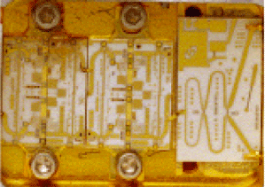
Fig. 1 MIC assembly on an open carrier.

Fig. 2 RF amplifier with several open-carrier blocks connected directly.
The connection of one carrier to another or to a transition line is supposed to be simple. A metal ribbon is connected to the signal line while the ground is assumed to be connected via the metal housing. Since everything is grounded and all metal parts are RF-grounded, the grounding regime is usually something that is taken for granted. It is only after problems such as low isolation or high gain ripple are observed that the ground regime is dealt with, usually by a process of trial-and-error. The most common practice is to push metal shims between the carrier and the housing. In the following study, several common connections are analyzed and compared. As a conclusion, some design rules are recommended.

Fig. 3 Supercomponent with several open-carrier blocks connected via transition lines.

Fig. 4 Model of the basic microstrip configuration for the refence problem.

Fig. 5 Reference problem port definition
Reference Problem
As a reference problem, two microstrip transmission lines were analyzed and the channel-to-channel isolation was simulated. The basic configuration is shown in Figure 4. The two transmission lines are implemented on an alumina substrate and separated by a row of via-holes. To simplify the simulation, the via-holes were replaced by a metallic wall. Each input or output of the transmission lines was assigned a port, as shown in Figure 5. For extracting all the information regarding the performance of the system in the complete frequency range from DC to 20 GHz, a time-domain simulation, using CST Microwave Studio,® was used. The system was injected with an input signal that has a very wide spectrum (see Figure 6), and the output signals were used to extract the frequency domain characteristics of the system. This is a fast method to analyze many frequency points very quickly. The first step of the simulation is to calculate the modes of each port. In this case, a quasi-TEM mode exists in all four ports. As expected, the electrical field lines are drawn from the signal (upper) conductor to the metal ground plane below. Other parameters, such as line impedance, are also extracted at this point.

Fig. 6 Reference problem; (a) time domain, (b) electric field distribution and (c) simulation results.

Fig. 7 Alumina-based filter connected to Teflon-based transmission lines.

Fig. 8 Model of a mmicrostrip-to-microstrip transition without carrier.
The simulation results demonstrate a very high isolation (46 dB min.) and good return losses (18 dB). These figures shall be used for comparison with the other simulations.
Microstrip Transition Study
The first case study is for two transmission lines on an alumina substrate connected to two transmission lines on a Teflon-based substrate (RTD 5880 by Rogers™). The alumina substrate is attached directly to the housing without any metal carrier. The Teflon-based substrate is also attached directly to the housing with a perfect metal wall between them. This situation is commonly used where the Teflon-based substrates are cut in any desirable shape and then soldered in special channels. The alumina is a hard and brittle ceramic, and is usually cut into simple rectangles and assembled in open-space areas. Such an example, an RF filter on an alumina substrate, is shown in Figure 7. This case is modeled accordingly and shown in Figure 8, where the two substrates are placed close to each other and there is no gap in the ground plane. This transition is expected to perform well since the ground regime is good. The port definition is similar to the reference problem and is shown in Figure 9. The simulation results are good and the isolation is 43 dB, which is slightly lower than in the reference case (see Figure 10).

Fig. 9 Port definitions for a microstrip-to-microstrip transition without carrier.
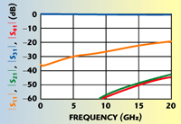
Fig. 10 RF performance of a microstrip-to-microstrip transition without carrier.
As previously discussed, the attachment of the building block into the supercomponent is usually done with carriers. To model this case, an air gap was introduced between the two substrates. The model is shown in Figure 11. The ground regime in this case is surely not optimal and the results are quite poor, as seen in Figure 12. The isolation dropped to 29 dB and the return loss dropped to 12 dB. These values are not acceptable in a supercomponent. High leakage from channel to channel, low out-of-band-rejection and high ripples are just some of the detrimental effects on system performance. Insight is possible when viewing the ground surface currents. As seen in Figure 13, the currents spread over a large section of the gap and the current of the left transmission line reaches the bottom of the right transmission line. This is the coupling mechanism from one transmission line to another. This effect is usually reduced by filling the gap with metal shims and epoxy adhesives.

Fig. 11 Model of a microstrip-to-microstrip transition with a carrier.

Fig. 12 RF performance of microstrip-to-microstrip transition with a carrier.

Fig. 13 Ground currents in a microstrip-to-microstrip transition with a carrier.

Fig. 14 Coplanar waveguide connections example.
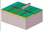
Fig. 15 Model of a coplanar-to-coplanar wavelength transition without a carrier.
Coplanar Waveguide Transition Study
The coplanar waveguide transmission lines are connected by three gold ribbons, one for the signal conductor and two for the ground plane (see the example in Figure 14). This case is illustrated in Figure 15. Note that via-holes are used in close proximity to the gap in order to connect the bottom ground plane to the upper ground plane, which is shown in Figure 16. First the electrical field distribution was simulated. The strong fields between the center conductor and the two ground planes is shown in Figure 17. From this result, it is concluded that the effects of the gap should not be strong. The simulation results of the case without a carrier (no air gap), shown in Figure 18, are excellent. The isolation is 53 dB and the return loss is 20 dB. These results are better than for the reference problem.

Fig. 16 Close view of via-holes in a coplanar-to-coplanar waveguide transition without a carrier.

Fig. 17 Electrical field in a coplanar-to-coplanar waveguide transition without a carrier.

Fig. 18 RF performance of a copplanar-to-coplanar waveguide transition without a carrier.


Fig. 19 RF perfomance of a coplanar-to-coplanar waveguide transition with a carrier.

Fig. 20 Microstrip-to-microstrip transition test fixture.

Fig. 21 Coplanar-to-coplanar transition test fixture.
By introducing the metal carrier, which means an air gap, the results drop slightly to an isolation of 46 dB and a return loss of 16 dB. The complete structure simulation results, shown in Figure 19, are quite surprising. The isolation in this case is still better than for the reference case.
Simulation Conclusions
The ground regime has a moderate effect on the return loss but a large effect on channel-to-channel isolation. Microstrip lines are extremely vulnerable to ground impairments, while coplanar waveguide lines are more tolerant. In Table 1, the isolation of the four simulated cases is compared.
From the above, several design rules are deduced:
• GCPWG-to-microstrip is preferred for transition implementations.
• Place via-holes close to the air gap.
• If microstrip must be used, do not use carriers.
• If microstrip with carriers must be used, add metallic walls to compensate for low isolation.

Fig. 22 Measured isolation for the microstrip transition.

Fig. 23 Measured isolation for the coplanar waveguide transition.
Measurement Results
In order to demonstrate the effects of the ground regime, two test fixtures were assembled. The test fixtures were designed to simulate a real life situation where some components are mounted on a metal carrier with some lines connected to it. The lines are realized as microstrip lines. To achieve good isolation in the test fixture, metal walls are placed in the sides of the lines. The isolation between the two channels is mainly affected by the body-to-carrier-to-body transition. The pure microstrip test fixture is shown in Figure 20. A second test fixture with coplanar-to-coplanar transition was realized. In this test fixture, the lines are still microstrip but the transition area was changed to coplanar. The second test fixture is shown in Figure 21.
The isolation was measured with these test fixtures and the isolation results are shown in Figures 22 and 23. While the microstrip transition yields an isolation of 16 dB at 18 GHz, the coplanar transition yields an isolation of 35 dB at the same frequency. This clear 20 dB advantage was expected in view of the simulation results. From the same figures, it can be observed that at all frequencies the isolation of the coplanar structure is about 20 dB better than for the microstrip structure, even at 500 MHz.
Acknowledgments
The photographs of the supercomponents and devices are courtesy of the Elisra Microwave Division, Israel (http://www.mw-elisra.com). The simulation software and support are courtesy of CST GmbH, Germany (http:// www.cst.com). Special thanks are given to Leonardo Sassi and Emmanuel Leroux from the CST support and sales teams.