
 In many quarters it is expected that Long Term Evolution (LTE) will be the next generation standard or the 3.9 generation (3.9G) mobile phone standard, which could be introduced as early as this year. The LTE advantage is a very high-speed data transfer capability of up to 326 Mbps and can utilize quite a few existing base stations, compared to other emerging high-speed data link systems such as WiMAX.
Key devices needed to realize longer talk time and lighter handsets are power amplifier modules (PAM). Because they consume a large amount of the current available from the power supply in a handset, it is essential to operate the PAM with high efficiency under the various modulation schemes.
In addition, it is important for the PAM to incorporate a simple digital input/output (I/O) interface and have reference voltage generation, as the reference voltage often plays an important role in the accurate bias feeding of HBT-based power amplifiers. The self-reference generation of the PAM allows a discrete low-voltage-drop-out regulator (LDO) to be removed on the printed-circuit board (PCB) and a digital I/O enables direct control of the PAM by advanced Si-based RF-LSIs or baseband LSIs. Thus, increased functionality as well as improved performance is a key requirement for the PAM.
BA012Dx Series
These requirements are more than satisfied by Mitsubishi Electric’s new BA012Dx series of power amplifier modules, which incorporate cutting-edge device and circuit technologies. These PAMs support current and near future cell phone handset applications from W-CDMA systems up to LTE systems. The applications include the latest fast data transfer systems—High Speed Downlink Packet Access (HSDPA), High Speed Uplink Packet Access (HSUPA) and High Speed Packet Access Plus (HSPA+).
The BA012Dx series has been specifically developed to address the requirements mentioned above and is a family of single-band PAMs for use in cell phone handsets or data cards for mobile applications. Compared to multi-band PAMs, the single-band PAM configuration gives customers the freedom for a more flexible PCB design. In the series, the BA012D1 is for band I, BA012D2 for band V, BA012D3 for band XI, BA012D4 for band II, BA012D5 for band VIII and BA012D6 for band III (IV). PAMs for other bands are currently being considered.
Integrated Coupler

Figure 1 Simplified block diagram of the BA012Dx (a) and gain/efficiency vs. Pout (b).
A block diagram of the PAM is shown in Figure 1. One of the key features is an integrated coupler for monitoring output power to simplify the layout of the handset. Other features are the integrated reference voltage generator and the control logic circuit, which address recent Si I/O level requirements. To achieve this level of integration, an advanced in-house BiFET technology has been employed for the BA012Dx series, which allows for both HBTs and FETs to be fabricated on the same die. In this process FET-based topologies can be used for the DC bias circuits and the analog RF switches, and these can be incorporated together with a conventional HBT power amplifier block. Thanks to the BiFET process, the BA012Dx series can be operated in three different power modes depending on the required output power level. These three power modes can be used to reduce the average current consumption and extend battery life. In the high power mode, the PAM works as a two-stage amplifier, delivering sufficient output power and linearity.
In contrast, the mid-power mode is implemented by switching the second stage off and bypassing it, leading to very high efficiency operation. In the low-power mode, only an additional small-size power stage is active while the other stages are kept in the off-state. As a result, the BA012Dx series is capable of delivering very high efficiency in each power mode.
Power-added Efficiency

Figure 2 Typical performance of the BA012Dx under W-CDMA modulation.
Figure 2 shows an example of the power measurement for the BA012D1 module under W-CDMA modulation test conditions. This PAM achieves power-added efficiencies (PAE) of 36 percent, 26 percent (or higher), and 10 percent in the high, mid, and low power modes, respectively, while maintaining adjacent channel leakage power ratio (ACLR) of less than -41 dBc and next adjacent channel leakage power ratio (NACLR) of less than -55 dBc.
Under the LTE (3rd Generation Partnership Project [3GPP] TS36.101) modulation condition of resource blocks (RB), 25 and 100, the PAEs of 31.3 and 31.4 percent can be achieved in the high power mode. The efficiency drop is minimized due to circuit parameter optimization for various modulation schemes from W-CDMA to LTE. The 3GPP compliant, probability distribution function (PDF)-based average current is as low as 27.7 mA, which is very effective in saving battery current consumption and consequently extending talk time in everyday cell phone use.

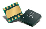
Figure 3 Cross-section view of a BA012Dx device.
The cross-section of a BA012Dx device is shown in Figure 3. The BiFET MMIC die is assembled on a small 3 × 3 mm glass epoxy substrate, together with several surface-mount devices (SMD) such as capacitors and inductors, used for matching and decoupling. The height of the package is less than 1 mm, which is suitable for realizing low-height cell phones and thin data cards.
Conclusion
Mitsubishi Electric has utilized the company’s wealth of manufacturing experience in producing very high reliability products to develop the BA012Dx series, which has been produced in order to satisfy the current and future mobile phone and data-card market requirements. Cutting-edge design and fabrication techniques have produced a range of PAMs that are expected to contribute to the realization of even smaller, lighter cell phone handsets.
Mitsubishi Electric Corp.
Tokyo, Japan
Tel: +81-3-3218-2111
Mitsubishi Electric Europe B.V.
Ratingen, Germany
Tel: +49-2012-486 0
RS No. 310