
Microstrip bandgap structures, such as photonic bandgap (PBG), electromagnetic bandgap (EBG) and defected ground structure (DGS), have recently been used to suppress high-order harmonics in antennas, amplifiers and oscillators1-4 because they are simple to fabricate and have excellent filtering performance. For example, Radisic1 introduced a wideband power amplifier using a dielectric PBG structure for higher harmonics suppression and improvement in power-added efficiency (PAE), while Lim2 reported a power amplifier with efficiency and output power improvements using a defected ground structure. However, slotted ground planes are required in the above-mentioned applications, which result in a large circuit size and higher insertion loss. Woo demonstrated that a single asymmetric slotted ground plane with compact size was excellent for second and third harmonics suppression simultaneously.5 Nevertheless, a slotted ground plane needs an etching process on the backside ground plane and an accurate position calibration, which increases cost and complexity.
A spurline structure is a simple slotted structure that is embedded directly into a microstrip line. Without any stubs and etch processing on the backside ground plane, it is a convenient process for dense integrated circuits because of their inherently compact design and ease of integration. Also, spurline structures can provide excellent bandgap characteristics and have been applied in antenna and filter designs.6,7 However, the reported spurline structures only provide a single bandgap to suppress one higher-order harmonic component.
Based on previous work about asymmetrical spurlines,8,9 a new method to suppress harmonics in a power amplifier is proposed, using an asymmetrical spurline structure. An asymmetrical spurline structure with dual rejection bands was designed and can be applied to the second and third harmonics suppression. Measured results are given and the improved output power and PAE performances of the power amplifiers are discussed.
Asymmetrical Spurline Structure and Power Amplifier Design

Figure 1 Layout of the proposed asymmetrical spurline structure.
An asymmetrical spurline structure is shown in Figure 1. It consists of two asymmetrical L-shaped slots embedded into the microstrip line. The length difference between the upper spurline and lower spurline is denoted by l. The configuration of the spurline structure is defined by three parameters: the slot width s, the slot length a and the slot height b. Because of the dimensional asymmetry, different inductance and capacitance effects of the asymmetrical spurline structure are expected and dual bandgap characteristics could be obtained.

Figure 2a Schematic of the power amplifier with the asymmetrical spurline structure.
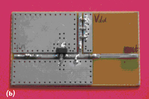
Figure 2b Photograph of the fabricated amplifier.
A MMIC InGaP HBT amplifier (HMC454ST89 from Hittite) combined with the proposed asymmetrical spurline structure is employed to realize a Class A power amplifier operating over the 1.7 to 2.2 GHz band. It is shown in Figure 2. The required drain bias voltage is set to +5 V. Choke inductors and shunt MIM capacitors are used in the bias circuit. The matching circuits are made of a microstrip impedance transformer, DC block capacitors and shunt capacitors. The asymmetrical spurline structure is etched in the output microstrip line to implement the second and third harmonics suppression. The proposed asymmetrical spurline structure’s dimensions are chosen as follows: s = 0.2 mm, a = 11.3 mm, l = 3.5 mm, b = 0.4 mm, w = 1.48 mm. A substrate with a relative dielectric constant of 4.5 and a thickness of 0.8 mm is used in the simulation and measurements. The amplifier circuit and the spurline patterns can be realized at the same time by a simple etching process.
The signals at the output of the amplifier are terminated by the asymmetrical spurline structure. Only the fundamental component F0 at 1.91 GHz passes through; the higher harmonic components (2F0 and 3F0) are suppressed, resulting in improved linearity and an increase in fundamental power.

Figure 3 Simulated amplifier performance.
In order to investigate the performance improvement of the amplifiers, two kinds of power amplifiers have been fabricated. One is a conventional design without the spurline structure, while the other is the proposed design. The simulated transmission characteristics of the amplifiers are shown in Figure 3. As shown, it is demonstrated that the optimum load impedance at the fundamental frequency (F0) is changed slightly after adding the asymmetrical spurline structure. Furthermore, it is found that the harmonics suppressions at the second and third harmonics are approximately 34.5 and 27 dB, respectively.

Figure 4 Measured performance of the two amplifiers: (a) power added efficiency (PAE) and (b) output power.
A comparison of the measured output power and PAE of the two amplifiers is shown in Figure 4. From the measured results, it is clearly observed that the asymmetrical spurline structure has improved the PAE of the power amplifier by 6 to 8 percent. Additionally, the improvement in output power is 0.4 to 1.0 dBm and is not appreciable because the magnitudes of the second and third harmonics are very small. The output power is improved by 1 to 4 percent.
Conclusion
A new method of adopting an asymmetrical spurline structure for higher harmonics rejection in microwave amplifiers is verified in this article. At the output of the proposed amplifier, an asymmetrical spurline structure with dual rejection bands is introduced to tune out the second and third harmonics. Compared to the conventional amplifier design, the asymmetrical spurline structure suppresses the second and third harmonics by more than 27 dB and yields an improved PAE by 6 to 8 percent. It is expected that the asymmetrical spurline structure can be widely used in other microstrip circuits and systems for tuning harmonics and improve performance while the design is compact and easy to integrate.
References
1. V. Radisic, Y. Qian and T. Itoh, “Broad Power Amplifier Using Dielectric Photonic Bandgap Structure,” IEEE Microwave and Guided Wave Letters, Vol. 8, No. 1, January 1998, pp. 13-14.
2. J.S. Lim, H.S. Kim, J.S. Park, D. Ahn and S. Nam, “A Power Amplifier with Efficiency Improved Using Defected Ground Structure,” IEEE Microwave and Wireless Components Letters, Vol. 11, No. 4, April 2001, pp. 170-172.
3. J.S. Lim, Y.C. Jeong, D. Ahn and S. Nam, “Improvement in Performance of Power Amplifiers by Defected Ground Structure,” IEICE Transactions on Electronics, Vol. E87-C, No. 1, January 2004, pp. 52-59.
4. H.J. Choi, J.S. Lim and Y.C. Jeong, “A New Design of Doherty Amplifiers Using Defected Ground Structure,” IEEE Microwave and Wireless Components Letters, Vol. 16, No. 2, December 2006, pp. 687-689.
5. D.J. Woo and T.K. Lee, “Suppression of Harmonics in a Wilkinson Power Divider Using Dual-band Rejection by Asymmetric DGS,” IEEE Transactions on Microwave Theory and Techniques, Vol. 53, No. 6, June 2005, pp. 2139-2144.
6. C. Nguyen and K. Chang. “On the Analysis and Design of Spurline Bandstop Filters,” IEEE Transactions on Microwave Theory and Techniques, Vol. 33, No. 12, December 1985, pp. 1416-1421.
7. W.H. Tu and K. Chang, “Compact Microstrip Bandstop Filter Using Open Stub and Spurline,” IEEE Microwave and Wireless Components Letters, Vol. 15, No. 4, April 2005, pp. 268-270.
8. H.W. Liu, L. Sun and Z. Shi, “Dual-bandgap Characteristics of Spurline Filter and Its Circuit Modeling,” Microwave and Optical Technology Letters, Vol. 49, No. 11, November 2007, pp. 2805-2807.
9. H.W. Liu, R. Cao, W. Hu and M. Wu, “Harmonics Suppression of Wilkinson Power Divider Using Spurlines with Adjustable Rejection Bands,” 2008 IEEE MTT-S International Microwave Symposium Digest, June 2008, pp. 189-192.
Haiwen Liu received his BS degree in electronic systems and his MS degree in radio and remote-sensing science from Wuhan University, Wuhan, China, in 1997 and 2000, respectively, and his PhD degree from Shanghai Jiao Tong University, China, in 2004. He is currently a professor with the School of Information Engineering, East China Jiaotong University, Nanchang, China. His main areas of research include radio system and microwave/RF IC design.
Fu Tong received his BS degree in microwave circuit and systems from the University of Electronic Science and Technology of China, Chengdu, China, in 2006. He is currently pursuing his master’s degree at the Institute of Optics and Electronics, Chinese Academy of Sciences (CAS), Chengdu, China.