
In view of the compact and portable nature of the wireless equipment, their compact size and configuration have been a big issue to the wireless industry. Some challenges in realizing miniaturized wireless antennas have been discussed by Cantrell1 and some new useful candidates using dielectric resonators and microstrips have been recently reported.2-4
Of all the possible structures investigated so far, microstrip appears to be the most advantageous for various reasons, including simplicity, cost, weight and fabrication. However, a microstrip patch having a rectangular or circular shape suffers from an inherent limitation of narrow impedance bandwidth (≈2 to 3 percent with VSWR < 2) and the peak gain is limited to 6 to 7 dBi. Several techniques are known to increase the impedance bandwidth of a microstrip antenna, but they usually reduce the antenna gain. Several gain enhancement techniques like using a planar array or superstrate layers are also known, but they could significantly reduce the antenna bandwidth.
In this work, the combination of some useful techniques have been explored to demonstrate a small size, high gain antenna with a considerably large impedance bandwidth accommodating a commercial wireless band. The techniques employed here were studied earlier by different groups individually to investigate a mechanically tunable patch,5,6 to compensate probe reactance7 and to study improved radiation properties using a shaped ground plane.8-11
Here, all of them have been employed in one structure for the first time, to realize a commercially viable high gain wireless antenna. As much as 11 dBi peak gain has been experimentally demonstrated using a prototype operating over the 1850 to 1990 MHz band (VSWR < 2 over 8 percent impedance bandwidth) for the PCS band. The antenna occupies only 0.15λ0 by 1.0λ02 space, λ0 being the wavelength corresponding to the center of the frequency band. The antenna, backed by a transmit-receive unit, can be packed together in a compact plastic enclosure and should be ideal for both indoor and outdoor installations. This is basically aimed to microcell applications to communicate with a base station as a booster/repeater device in a weak signal zone like an airport, large building, shopping mall, etc.
Design Approach

Figure 1 Schematic diagram of the proposed wireless antenna.
A schematic diagram of the antenna is shown in Figure 1. A coaxial-fed circular patch, etched on a microstrip substrate, is used as the radiating element where the substrate is fitted within a circular cylindrical cavity having its diameter D equal to approximately the resonant wavelength and the depth l ≈0.15D. The substrate maintains a variable air gap h with the ground plane, which is the floor of the metal cavity. An annular slot is introduced surrounding the feed point. This design approach, aimed at achieving a high gain performance over a wide impedance bandwidth using a compact ground plane, is provided below:
(i) An increase in the substrate thickness and decrease in its relative permittivity are two suitable choices to enhance the impedance bandwidth of a microstrip patch. This was implemented by introducing an air gap below the substrate.5,6 In the original work with an air gap,5 the objective was to tune the antenna by varying the gap height h. In the present structure, the air gap results in increased electric fringing fields; hence, a considerable increment in the effective radius of the radiating patch is obtained, which can be estimated.6 This increment in the effective patch radius causes the enhancement in the antenna gain.
(ii) Feeding through a coaxial probe has been chosen since it is simple, less expensive and efficient for integrating with the transceiver front end. However, the long center conductor penetrating through the substrate with air gap results in a large value of feed inductance, which degrades the impedance matching at the input. A capacitive loading by an annular slot on the patch, surrounding the feed, was demonstrated by Hall7 as a probe compensation technique for a thick substrate. Here, for the first time, that technique has been applied to the proposed geometry with an air-gap to simultaneously achieve the high gain along with a wide matching bandwidth.
(iii) Maintaining the ground plane size as small as possible is another requirement for a compact wireless antenna, which in turn, for a microstrip element, degrades the radiation pattern and the antenna gain. This aspect has been taken care of by introducing a metal cavity surrounding the patch, which also prevents diffraction at the edge of the ground plane. Some earlier studies employing cavity and shaped ground plane8-11 also addressed the possibility of reduction in patch size and improvement in radiation characteristics.
For the present design, the optimum parameters like the patch radius a, the air gap h and the feed location c have been directly calculated from previously published formulas,6,12 for the center frequency of the band. The antenna has been designed to operate over an approximately 8 percent matching bandwidth; the matching parameters r and s of the annular slot have been optimized through a series of simulation studies.13 The other important parameters like the cavity diameter D and depth l were thoroughly studied in view of achieving optimized radiation properties. Further details of the design parameters are also available.14
Measured and Simulated Results
A prototype, operating in the PCS band, was fabricated and measured using an HP 8510 B network analyzer and a fully automated anechoic chamber. Some representative results are presented. Figure 2 shows the measured and simulated return loss characteristics of the prototype. The antenna parameters are: εr = 4.5, t = 1.575 mm, l = 25 mm, d = 1.275 mm, a = 33 mm, r = 5 mm, s = 0.8 mm, c = 14 mm, h = 5 mm and D = 160 mm. The measurements show close agreement with the optimum simulated return loss values. The measured S11 values rather indicate a comparatively improved impedance matching at the antenna input.

Figure 2 Measured and simulated return loss of the prototype antenna.

Figure 3 Simulated radiation patterns for different heights of the cavity wall: (a) E-plane and (b) H-plane.
The diameter of the ground plane has been initially chosen to be approximately 1.0λ0 (D ≈ 160 mm). The effect of the cavity height l on the radiation characteristics has been examined and is shown in Figure 3. Those corresponding to l = 25 mm indicate the best possible response in view of the optimum beam shape and minimum backward radiation. The effect of change in D value above and below D = 160 mm has also been examined and is shown in Figure 4, keeping l = 25 mm. A decrease in D by 20 mm (that is D = 140 mm) results in relatively 1 dB down in the peak gain. Again, an increase of D by 20 mm (D = 180 mm) is found to enhance the peak gain by approximately 1 dB, but with a considerable back radiation, particularly in the E-plane pattern. Therefore, D = 160 mm with l = 25 mm appears to be the best choice to achieve a good radiation pattern with an optimum peak gain of approximately 11 dBi.

Figure 4 Simulated radiation pattern for different cavity diameters.
Figure 5 shows the measured values of the peak gain along with the simulated data. The simulated data have been generated in two sets: over 1.85 to 1.9 GHz, using 1.9 GHz as the ‘solution frequency’, and over 1.92 to 2 GHz, using 2 GHz as the ‘solution frequency’. The simulation shows close agreement with the measurements indicating a maximum relative deviation of the order of 0.5 dB.

Figure 5 Measured and simulated peak gain of the prototype antenna.
The measured radiation characteristics of the PCS antenna are shown in Figure 6 near the centers of its two sub-bands called uplink (1.85 to 1.91 GHz) and downlink (1.93 to 1.99 GHz) frequencies. Both the co- and cross-polarized patterns at these two frequencies are identical. As much as 11 dBi peak gain with its main lobe aligned to the bore sight is revealed. The simulated gain, shown previously, closely corresponds to the measured values except for the E-plane cross-polarized level. Though no significant cross-polarized radiation above -25 dB is obtained theoretically, the measurements show this as much as -10 dB near bore sight. Such an experimental observation was also indicated and discussed in a previous paper.15
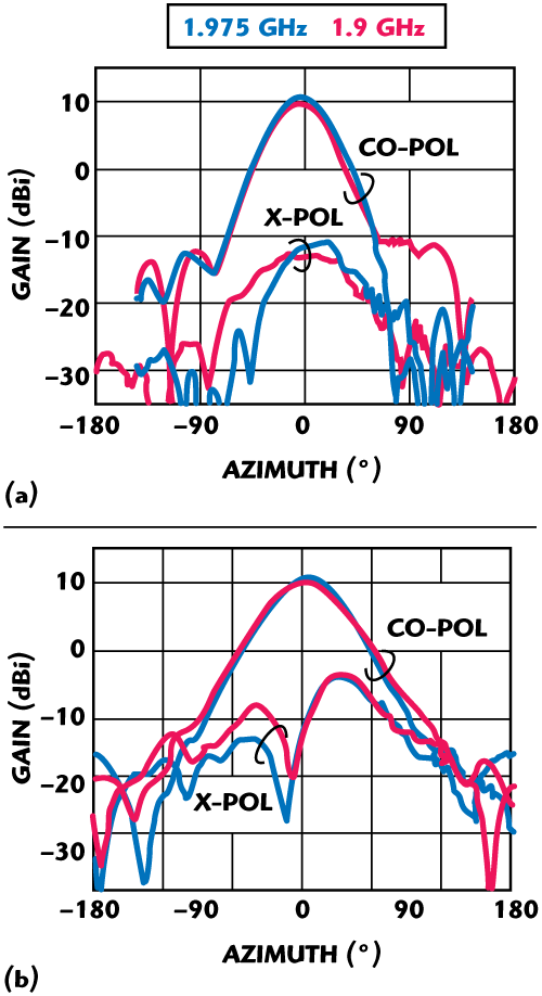
Figure 6 Measured radiation characteristics of the proposed antenna: (a) E-plane and (b) H-plane.
Conclusion
A new design of an antenna suitable for certain wireless applications is presented. The performance of the antenna is demonstrated based on theoretical and experimental studies. This antenna is simple, less expensive, compact in size and with relatively high gain, operating over the PCS frequencies. As much as 11 dBi peak gain with linear polarization and 8 percent impedance bandwidth have been experimentally demonstrated.
References
1. W.H. Cantrell, et al., “PCS Antenna Design: The Challenge of Miniaturization,” IEEE Antennas and Propagation Magazine, Vol. 43, No. 4, August 2001, pp. 12-27.
2. D. Guha and Y.M.M. Antar, “Four-element Cylindrical Dielectric Resonator Antenna for Wideband Monopole-like Radiation,” IEEE Transactions on Antennas and Propagation, Vol. 54, No. 9, September 2006, pp. 2657-2662.
3. L.C.Y. Chu, D. Guha and Y.M.M. Antar, “Air Gap Loaded Ultra Wideband Dielectric Resonator Antenna for Commercial Wireless Bands,” International Symposium on Antenna Technology and Applied Electromagnetics & Canadian Radio Sciences (URSI/CNC), Montreal, Canada, July 2006.
4. D. Guha, et al., “Novel High Gain Wireless Antenna for PCS Band,” IEEE Radio and Wireless Symposium, January 2007, Orlando, FL.
5. K.F. Lee, K.Y. Ho and J.S. Dahele, “Circular Disc Microstrip Antenna with an Air Gap,” IEEE Transactions on Antennas and Propagation, Vol. 32, No. 8, August 1984, pp. 880-884.
6. D. Guha, “Resonant Frequency of Circular Microstrip Antennas with and without Air Gaps,” IEEE Transactions on Antennas and Propagation, Vol. 49, No. 1, January 2001, pp. 55-59.
7. P.S. Hall, “Probe Compensation in Thick Microstrip Patches,” Electronics Letters, Vol. 23, No. 11, May 1987, pp. 606-607.
8. F. Zavosh and J.T. Aberle, “Single and Stacked Circular Microstrip Patch Antennas Backed by a Circular Cavity,” IEEE Transactions on Antennas and Propagation, Vol. 43, No. 7, July 1995, pp. 746-750.
9. N.C. Karmakar, “Investigations into a Cavity-backed Circular-patch Antenna,” IEEE Transactions on Antennas and Propagation, Vol. 50, No. 12, December 2002, pp. 1706-1715.
10. D. Guha and J.Y. Siddiqui, “Effect of a Cavity Enclosure on the Resonant Frequency of Inverted Microstrip Circular Patch Antennas,” IEEE Transactions on Antennas and Propagation, Vol. 52, No. 8, August 2004, pp. 2177-2180.
11. S. Noghanian and L Shafai, “Control of Microstrip Antenna Radiation Characteristics by Ground Plane Size and Shape,” IEEE Proceedings on Microwaves, Antennas and Propagation, Vol. 145, No. 3, June 1998, pp. 207-212.
12. D. Guha, Y.M.M. Antar, J.Y. Siddiqui and M. Biswas, “Resonant Resistance of Probe and Microstrip Line-fed Circular Microstrip Patches,” IEEE Proceedings on Microwaves, Antennas and Propagation, Vol. 152, No. 6, December 2005, pp. 481-484.
13. High Frequency Structure Simulator (HFSS), Ansoft, v 10.1.
14. D. Guha, Y.M.M. Antar and P. Beland, US Patent Appl. No. 11/740,517, 2007.
15. D. Guha, M. Biswas and Y.M.M. Antar, “Microstrip Patch Antenna with Defected Ground Structure for Cross Polarization Suppression,” IEEE Antennas and Wireless Propagation Letters, Vol. 4, 2005, pp. 455-458.