
Recently, the demand for highly integrated and miniaturized radio frequency integrated circuits (RFIC) has increased in the wireless communication systems market. With the evolution of silicon CMOS device process technology, highly integrated silicon ICs, including RF and base-band block, have been developed.1 However, passive components such as couplers, dividers and filters are fabricated outside the ICs due to their large sizes, which have been an obstacle in the realization of fully-integrated silicon front-ends. To solve this problem, a short wavelength transmission line, applicable to the development of miniaturized passive components on silicon substrate, must be developed. To date, using a photonic band gap (PBG) structure, a number of miniaturized passive components have been fabricated on GaAs and Teflon substrates.2,3 However, short wavelength transmission lines and miniaturized passive components on silicon substrates have not yet been studied. The study of silicon passive components has instead been focused on the development of low loss structures, such as patterned ground shield (PGS), due to the high conductivity of silicon substrates.4
In this work, in order to realize highly miniaturized passive components on silicon RFICs, a coplanar waveguide employing a periodically arrayed grounded-strip structure (PAGS) is proposed for the first time. Using the coplanar waveguide employing PAGS, a highly miniaturized branch-line coupler was developed for U-band silicon RFIC applications. This work is the first report of an on-chip coupler/divider employing transmission lines with a periodic structure on silicon substrate.
A Short Wavelength Coplanar Waveguide Employing PAGS
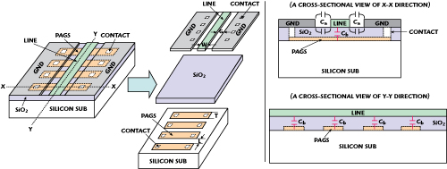
Figure 1 Structure of the coplanar waveguide using PAGS.
Figure 1 shows the structure of the coplanar waveguide employing PAGS. As shown, the PAGS exists at the interface between the SiO2 film and the silicon substrate, and is electrically connected to the top-side ground planes (GND planes) through via contacts. As is well known, a conventional coplanar waveguide, without PAGS, has only a periodical capacitance Ca per unit length, while the coplanar waveguide employing PAGS has an additional capacitance Cb as well as Ca due to PAGS. As shown, Cb is the capacitance between the line and PAGS. In other words, the total capacitance (per unit length) of the coplanar waveguide employing PAGS is Ca + Cb, but only Ca for a conventional coplanar waveguide without PAGS. Therefore, the coplanar waveguide employing PAGS exhibits a guided wavelength (λg) much shorter than a conventional one, because λg is inversely proportional to the periodic capacitance, i.e. λg = 1/[f(LC) 0.5].
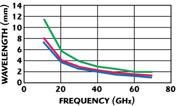
Figure 2 Measured wavelength of CPWs using PAGS and a conventional one.
Figure 2 shows the measured wavelengths of the coplanar waveguide employing PAGS and the conventional one. The coplanar waveguides were fabricated on a silicon substrate with a height of 600 µm. L and W are both 20 µm, and the thickness of the SiO2 film is 1 µm. The red and blue lines correspond to the data of the PAGS with a T of 5 and 20 µm, respectively. The green line is for the conventional CPW. As shown, the wavelength of the coplanar waveguide was reduced from 60 to 65 percent of the conventional one by using PAGS. For example, the wavelength for the coplanar waveguide employing PAGS (with a T of 20 µm) is 3.7 mm at 20 GHz, while the wavelength for the conventional coplanar waveguide without PAGS is 5.9 mm at the same frequency. The above results indicate that highly miniaturized passive circuits can be realized by using the coplanar waveguide employing PAGS.
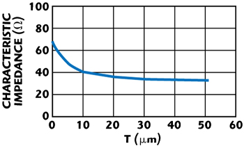
Figure 3 Measured characteristic impedance of the coplanar waveguide using PAGS.
The measured characteristic impedance of the coplanar waveguide employing PAGS is shown in Figure 3, where line width W was fixed to a value of 20 µm. As T becomes larger, the characteristic impedance becomes lower, because the characteristic impedance is inversely proportional to the periodical capacitance of the transmission line, i.e. Z0 = (L/C)0.5. An increase in T results in an enhancement of periodical capacitance Cb due to an increase in the capacitive area. For this reason, the characteristic impedance of the coplanar waveguide employing PAGS can be easily controlled by only changing T. Using PAGS, the characteristic impedance can be reduced to a value much lower than for a conventional coplanar waveguide. For example, the characteristic impedance shows a value of 67 to 32 Ω when T varies from 0 to 50 µm. This characteristic is very favorable to a reduction of size of passive components on RFIC, because a very low impedance line is required for impedance matching between active devices. In other words, the input/output impedance of FETs are much lower than 50 Ω (10 to 40 Ω) in the RF band,5 and a very low impedance line should be used for impedance matching between FETs.
For example, the line width W of a conventional coplanar waveguide (having a G of 30 µm) with a characteristic impedance of 35 Ω is 130 µm, while the line width W of a coplanar waveguide using PAGS (having a T of 20 µm) with the same characteristic impedance is only 20 µm. Therefore, if a coplanar waveguide employing PAGS is used for impedance matching between active devices with low impedance, the line width W can be highly reduced (by only adjusting T), compared with a conventional coplanar waveguide.
Highly Miniaturized Branch-line Coupler Employing PAGS on Si Substrate

Figure 4 Photograph of the branch-line coupler using PAGS on a silicon substrate.
Using the coplanar waveguide employing PAGS, a highly miniaturized branch-line coupler was developed for U-band RFIC applications. Figure 4 shows the branch-line coupler fabricated on a silicon substrate. The GSG pads were connected to the input and output ports for on-wafer measurement; the branch-line coupler corresponds to the area surrounded by a dotted line. Three samples were prepared for the measurements of S21, S31 and S41. The unused ports were terminated with 50 Ω thin film resistors. Because the port impedance is 50 Ω, the characteristic impedances of the two lines comprising the branch-line coupler are 50 and 35 Ω, respectively. In order to realize the coplanar waveguide with 50 and 35 Ω, the value of T was set to 5 and 20 µm, respectively. The lengths of the λ/4 lines comprising the branch-line coupler were determined from the measured waveguide length, described before.
In the case of a center frequency of 46 GHz, the size of the branch-line coupler employing PAGS was 0.46 × 0.55 mm, which is 37 percent of the size of the one fabricated by a conventional coplanar waveguide. In other words, in the case where the branch-line coupler is fabricated with a conventional coplanar waveguide (having a G of 30 µm) on a silicon substrate with a height of 600 µm, the length of the λ/4 line is 0.54 mm at a center frequency of 46 GHz, the widths W of the coplanar waveguide with a characteristic impedance of 50 and 35 Ω are 60 and 130 µm, respectively. Therefore, the size of the branch-line coupler employing a conventional coplanar waveguide is 0.9 × 0.76 mm.
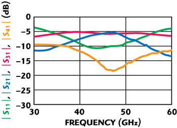
Figure 5 Measured power division, isolation and return loss characteristics of the branch-line coupler using PAGS.

Figure 6 Measured phase difference between S21 and S31 for the branch-line coupler using PAGS.
Figure 5 shows the power division, the isolation and return loss characteristics of the branch-line coupler employing PAGS. A good power division characteristic can be observed from 41.75 to 50 GHz. Specifically, S21 and S31 exhibit a value of 5.7 dB at 46 GHz. In the frequency range from 41.75 to 50 GHz, S21 and S31 show a value of 5.9 ± 0.5 and 5.5 ± 0.5 dB, respectively. Actually, the power division value for a branch-line coupler fabricated on a Teflon substrate6 is approximately 5 ± 0.5 dB, and the branch-line coupler employing PAGS shows a loss higher by 0.7 dB than for a conventional one, which originates from the high conductivity silicon substrate. The isolation characteristic (S41) shows a value of 18.1 dB at 46 GHz, and a value of 13 to 18.1 dB in the frequency range from 41.75 to 50 GHz. All ports show the same return loss due to the symmetry of the structure, and only S11 was plotted in the figure. S11 shows a value of 11.1 dB at 46 GHz, and lower than 10 dB in the frequency range from 41.75 to 50 GHz. Figure 6 shows the phase difference between S21 and S31 for the branch-line coupler employing PAGS. The phase difference shows a value of 90.1° at 46 GHz, and a value of 90 ± 4.8° in the frequency range from 41.75 to 50 GHz.
Conclusion
A coplanar waveguide employing PAGS exhibits a wavelength much shorter than a conventional one. Using the coplanar waveguide employing PAGS, a highly miniaturized branch-line coupler was fabricated on a silicon substrate for U-band RFIC applications. The branch-line coupler shows good RF performance from 41.75 to 50 GHz and its size is 0.46 × 0.55 mm, which is 37 percent of the size of the one fabricated by conventional coplanar waveguide. This work is the first report of an on-chip coupler/divider employing transmission lines with periodic structure on silicon substrate.
Acknowledgment
This research was supported by the Ministry of Knowledge Economy (MKE), Korea, under the Information Technology Research Center (ITRC) support program supervised by the National IT Industry Promotion Agency (NIPA). This work was financially supported by the Ministry of Knowledge Economy and the Korea Industrial Technology Foundation (KOTEF) through the Human Resource Training Project for Strategic Technology.
References
1. M. Zargari and D. Su, "Challenges in Designing CMOS Wireless Systems-on-a-Chip," IEICE Transactions on Electronics, Vol. E90-C, No. 6, June 2007, pp. 1142-1148.
2. F.R. Yang, K.P. Ma, Y. Qian and T. Itoh, "A UC-PBG Structure and Its Applications for Microwave Circuits," IEEE Transactions on Microwave Theory and Techniques, Vol. 47, No. 8, August 1999, pp. 1509-1514.
3. Y. Yun, K.S. Lee, C.R. Kim, K.M. Kim and J.W. Jung, "Basic RF Characteristics of the Microstrip Line Employing Periodically Perforated Ground Metal and Its Application to Highly Miniaturized On-chip Passive Components on GaAs MMIC," IEEE Transactions on Microwave Theory and Techniques, Vol. 54, No. 10, October 2006, pp. 3805-3817.
4. Y.S. Lin. C.C. Chen, H.B. Liang, T. Wang and S.S. Lu, "Characterization and Modeling of Pattern Ground Shield and Silicon-substrate Effects on Radio-frequency Monolithic Bifilar Transformers for Ultra-wideband Radio-frequency Integrated Circuit Applications," Japanese Journal of Applied Physics, Vol. 46, No. 1, January 2007, pp. 65-70.
5. Y. Yun, M. Nishijima, M. Katsuno, H. Ishida, K. Minagawa, T. Nobusada and T. Tanaka, "A Fully-integrated Broadband Amplifier MMIC Employing a Novel Chip Size Package," IEEE Transactions on Microwave Theory and Techniques, Vol. 50, No. 12, December 2002, pp. 2930-2937.
6. I. Bahl and P. Bhartia, Microwave Solid State Circuit Design, Chapter 4, John Wiley & Sons Inc., New York, NY, 1988.