
The DC IV characterization of a device is important in predicting RF operation. DC IV results predict the quiescent bias and low frequency IV characteristics for a device, while in some cases they can be corrected to represent RF characteristics at a given quiescent bias point.1,2 In addition, they can be used in measurement of the thermal resistance of a device3 and analysis of the type and time-dependence of processes present in a device.4 In using static DC IV measurements for these applications, it is assumed that the dwell time in each region is sufficiently long for device thermal and trapping processes to reach steady state at each point measured. If this is not the case, the true DC IV results may not be achieved, but a set of IV curves where each measured data point has an incorrect thermal and/or trapping dependence is obtained. In the experiment presented herein, the dependence of the results on the delay factor in IV measurements made using a Keithley 4200 DC parameter analyzer is explored for GaAs MESFET and Si MOSFET example devices. It is found that for the GaAs device that has significant trapping effects apparently possessing long time constants, the accuracy of the static IV curves is compromised if the delay time is too low. However, for the Si MOSFET, the lowest delay factor setting (fastest sweep) can be used with excellent accuracy.
Thermal and Trapping Processes
Thermal and trapping effects have been shown to play a part in the measurement of static IV curves.5–7 These effects are known as “slow processes” and do not have time to occur in RF operation due to the short dwell time at each signal location; hence, pulsed IV measurement methods are often used to find the “RF IV” curves. DC IV curves, however, are still necessary in applications where the quiescent bias point is not known or is changing, such as in class B, AB, E, or F operation. In static DC IV measurement, it is necessary that the slow processes have time to reach steady state at each measurement point. This can be accomplished if the sweep rate of the curve tracer is low enough that the dwell time in each measurement region is sufficiently higher than the time constant of the effect. In other instruments, which do not sweep the curves but perform steps between points, the incorporation of a delay between measurements allows the device to remain biased at each point for a longer period of time.
How long does the dwell time in each region need to be? Walker gives an approximate room-temperature time constant of a thermal effect as 156 ms,8 while Ladbrooke and Bridge conclude that thermal time constants can lie in the tens of microsecond range.9 This means that the (VGS, VDS) bias of the device must remain in the same region longer than this length of time to provide an accurate measurement. Some trapping processes are even slower, stated to be on the order of milliseconds.7 Thus, the bias placed on the device must be in the region of measurement a minimum time of 0.1 to potentially even on the order of 100 milliseconds, depending on the device and its effects, before a measurement is performed.
The Normalized Difference Unit
For many years, sets of current-voltage (IV) curve data have been compared qualitatively. The degree to which the sets of IV curves are correlated is often determined by visual inspection in which it is determined that the curves either match well or deviate unacceptably. Quantitative comparison provides a method of numerical analysis of IV curve differences and the ability to plot the differences in the IV curves versus a variable (such as sweep rate). The normalized difference unit, which can be used for such comparisons, is defined as2,4

where IDS1i and IDS2i are the drain-source current values at the ith (VGS,VDS) points of measurement on the two current-voltage characteristics and IDSmean is the average of the current values over all measured points from both characteristics:
![]()
While this unit can be used to compare virtually any two sets of IV data for the same device, it is used to compare static DC IV data obtained using different delay settings in this experiment.
Experimental Results
To examine the variation of IV measurements with dwell time and sweep rate, the DC IV characteristics of a commercial 1 W GaAs MESFET and a 7 W power Si MOSFET were measured using a Keithley 4200 Semiconductor Characterization System. The dwell time in each region during measurement was altered by adjusting the instrument delay factor (DF) to values ranging from 1 to 100. The delay factor is multiplied by a base delay time of 4.5 milliseconds to obtain the total delay time before the data is acquired at each measurement point. The NDU was used to compare the IV data measured for each DF setting to the IV curves measured for DF = 100 (delay time = 450 ms), the largest DF used in the experiment.
For the GaAs MESFET, the settings used were as follows:
Gate Forcing Function: Voltage Step

Drain Forcing Function: Voltage Sweep

A DC IV measurement was performed with the above settings for delay factors of 1, 2, 5, 10, 20, 50 and 100. A filter factor of 1 was used, meaning that the base data acquisition time of 8 ms per data point is used for all measurements. Before the data is acquired, a delay time of 4.5 ms (the base delay time) multiplied by the delay factor is enforced. From observation, it appeared that the delay factor of 100 with a step size of 0.05 V yielded a sweep rate of approximately 0.1 V/s, which coincides with the rate estimated using the delay and filter factors. Similarly, use of a DF = 1 setting can be estimated to result in a sweep rate of approximately 4 V/s. For higher delay factors, the overall measurement time was significantly larger than for low delay factors, matching these expectations.
First, the repeatability of the instrument was measured by using the NDU to compare IV curves for identical DF settings. Averaging the NDU comparisons of identical measurements with DF = 1, 10 and 100 provides a repeatability noise floor of NDU = 9.98 ¥ 10–4, or approximately 0.001.
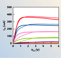
Fig. 1 Comparison of the GaAs MESFET IV curves for DF=100 (solid curves) and DF=1 (dashed curves) at NDU=0.065.
An examination of the IV curves shows a marked difference between the results obtained for DF = 1 and DF = 100 (see Figure 1). The NDU value expressing the difference between these results is 0.065. The largest differences in these results appear to be in the knee region and for high values of VDS in the upper curves. The knee region discrepancies are suspected to be due to trapping effects, as has been seen in previous experimentation by the authors. The discrepancies in the upper curves for large drain voltage are likely due to differences in self-heating in the devices at the time of measurement.7 Figure 2 shows that the difference between the DF = 50 curves and the DF = 100 curves is much lower (NDU = 0.005835).

Fig. 2 Comparison of the GaAs MESFET IV curves for DF=100 (solid curves) and DF=50 (dashed curves) at NDU=0.005835.
As previously noted, a delay factor of 1 on the Keithley instrument corresponds to a delay time of approximately 4.5 ms. Thus, a delay factor of 50, for which good results are obtained, is estimated to correspond to a delay time of 225 ms. While this seems like a long time for trap effects to reach steady state, it is quite consistent with the estimate of milliseconds for a time constant given in Reference 10 for trap effects. In addition, the GaAs MESFET used in this experiment does not have a gate recess, which tends to cause increased surface-state trap effects.10
For each DF setting, the NDU was computed between the IV curves resulting from that DF setting and the DF = 100 curves (the measurement with the longest delay). The values of NDU are plotted against the delay factor value in Figure 3, showing that the difference between the curves decreases (and hence the accuracy of the DC IV measurement increases) with increasing delay factor. The measurement repeatability line of NDU = 9.98 ¥ 10–4 is also shown. It is interesting to note that the NDU value approaches the repeatability NDU as the DF is increased.
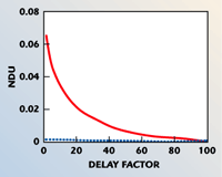
Fig. 3 NDU versus delay factor, comparing each measurement (solid line) and instrument repeatability NDU (dashed line).
This illustrates that for the “normal” setup with filter factor = 1 and delay factor = 1, an accurate static DC IV measurement is not obtained for this device. However, obtaining the set of curves for DF = 100 takes on the order of three to five minutes.
The same experiment was repeated for the Si MOSFET. In this case, a large difference was not noticed between the results. The NDU comparing the DF = 1 to DF = 100 IV curves is a mere NDU = 0.011, while the average instrument repeatability NDU is 0.00278 for the MOSFET. The DF = 1 and DF = 100 curves are shown in Figure 4. It is evident that the curves show no large difference. In fact, the dashed curves, which represent the DF = 1 setting, are actually lower than the DF = 100 curves, which should not be the case according to observed results concerning MOSFET device self-heating.2 The NDU versus DF plot is given in Figure 5. It can be seen that while a decrease is observed with increasing DF, the magnitude of the NDU is low for all DF settings, just above the repeatability level. Therefore, it is concluded that this difference may be due to measurement conditions (such as, “How warm is the device from the last measurement?”). The measurements for the LDMOS FET were made in order from DF = 1 to DF = 100. To gain insight into this, it could be advantageous to repeat the experiment, randomizing the order in which these measurements are taken, and observing whether the NDU versus DF graph changes. It appears from the results of this experiment that measuring with too small of a delay factor would have the largest detriment in the GaAs MESFET measurement, while little compromise in accuracy would occur in the case of the Si MOSFET.

Fig. 4 Comparison of the Si MOSFET IV curves for DF==100 (solid curves) and DF=1 (dashed curves) at NDU=0.011.

Fig. 5 NDU versus delay factor for the MOSFET device.
Conclusion
The use of a sufficiently long sweep rate may be necessary to achieve an accurate static DC IV measurement. If the sweep rate used is too fast, thermal and trapping processes, if present, might not reach steady state in the region of measurement for each measurement point. However, in device operation at a quiescent bias point or at a low frequency, steady-state thermal and trapping conditions are generally held at the conditions that exist at the bias point. From the results presented in this article, it is apparent that for the case of Keithley 4200 DC IV measurements a delay factor of 20 or so was sufficient for accurate measurement results on the Si MOSFET device example, while for the GaAs MESFET example, a delay factor of greater than about 80 was required. The presented NDU metric is a useful tool to use in comparing IV curves in simple studies like this one to help confirm the appropriate instrument settings to use for a given device type. n
Acknowledgments
The authors would like to thank Lee Stauffer of Keithley Instruments for his very helpful suggestions. It is also gratefully acknowledged that this work was sponsored in part by a fellowship grant from the Automatic RF Techniques Group (ARFTG).
References
1. C. Baylis, L. Dunleavy and J. Daniel, “Thermal Correction of IV Curves for Nonlinear Transistor Modeling,” IEEE Wireless and Microwave Technology Conference, Clearwater, Florida, April 2004.
2. C. Baylis, “Improved Current-voltage Methods for RF Transistor Characterization,” Master’s Thesis, University of South Florida, April 2004.
3. C. Baylis, L. Dunleavy and J. Daniel, “Measurement of Thermal Circuit Parameters Using Pulsed IV and the Normalized Difference Unit,” IEEE MTT-S International Microwave Symposium Digest, June 2004.
4. C. Baylis, L. Dunleavy and A. Snider, “The Normalized Difference Unit as a Standard Metric for Comparing IV Curves,” 64th Automatic RF Techniques Group Conference, Orlando, FL, December 2004.
5. A. Platzker, A. Palevsky, S. Nash, W. Struble and Y. Tajima, “Characterization of GaAs Devices by a Versatile Pulsed I-V Measurement System,” IEEE MTT-S International Microwave Symposium Digest, Vol. 3, 1990, pp. 1137–1140.
6. J. Scott, J. Rathmell, A. Parker and M. Sayed, “Pulsed Device Measurements and Applications,” IEEE Transactions on Microwave Theory and Techniques, Vol. 44, No. 12, December 1996, pp. 2718–2723.
7. L. Dunleavy, W. Clausen and T. Weller, “Pulsed IV for Nonlinear Modeling,” Microwave Journal, Vol. 46, No. 3, March 2003, pp. 68–84.
8. J.L.B. Walker, High Power GaAs FET Amplifiers, Artech House Inc., Norwood, MA, 1993.
9. P. Ladbrooke and J. Bridge, “The Importance of the Current-voltage Characteristics of FETs, HEMTs and Bipolar Transistors in Contemporary Circuit Design,” Microwave Journal, Vol. 45, No. 3, March 2002, pp. 106–120.
10. P. Ladbrooke, “Pulsed I(V) Measurement of Semiconductor Devices,” Accent Optical Technologies, 2004.
Charles Baylis received his BSEE and MSEE degrees from the University of South Florida (USF) in 2002 and 2004, respectively, and is presently a PhD student and adjunct instructor in the department of electrical engineering at USF, specializing in microwave transistor modeling and measurements. His master’s thesis, “Improved Current-voltage Methods for RF Transistor Characterization,” investigates the application of pulsed IV measurements toward accurate electrothermal RF characterization and was recognized with a 2004 Outstanding Thesis Award by the USF Graduate School. He is also a recipient of the 2004 Automatic RF Techniques Group (ARFTG) Microwave Measurement Student Fellowship. He has authored several papers regarding IV techniques and numerical comparison of data for transistor characterization.
Lawrence Dunleavy received his BSEE degree from Michigan Technological University in 1982, his MSEE and PhD degrees from the University of Michigan in 1984 and 1988, respectively, and was a Howard Hughes Doctoral Fellow (1984–1988). He worked for E-Systems (1982–1983) and Hughes Aircraft Co. (1984–1990) before joining the University of South Florida in 1990. He is currently a professor in the department of electrical engineering and the co-founder of the University of South Florida’s Center for Wireless and Microwave Information Systems. In 2001, he co-founded Modelithics Inc., a company involved in RF and microwave component and IC modeling solutions and related measurement services. He is a senior member of IEEE, and is very active in both the IEEE MTT Society and the Automatic RF Techniques Group (ARFTG).
William Clausen received his BSEE and MSEE degrees from the University of South Florida in 2003. Since 2002, he has been an engineer for Modelithics Inc., where he is currently involved in active device characterization and modeling. His active interests include high power, linear and noise modeling of transistors, as well as modeling solutions for new design applications.