
A 90° power combiner has been used for signal mixing at the intermediate frequency (IF) output port of an image rejection mixer.1,2 Until now, a passive branch-line coupler was mainly employed for 90° power combining.1,3 However, the passive branch-line coupler occupies a very large circuit area.
For example, if the branch-line coupler is fabricated on a GaAs substrate with a thickness of 100 µm, for a signal mixing with an IF of 2.4 GHz, the size will be approximately 10.92 × 10.54 mm. Therefore, passive power combiners cannot be integrated on MMICs due to their very large size.4 To reduce the size of the 90° power combiner,6 it has to be fabricated using an active device. However, no study of a 90° power combiner employing an active device has been reported yet. In this work, for integration of the 90° power combiner on a MMIC, a highly miniaturized active 90° power combiner employing CE and CC circuits with InGaP/GaAs heterojunction bipolar transistors (HBT) is proposed.
Design of An Active 90° Power Combiner Employing CE and CC with InGaP/GaAs HBT

Figure 1 Schematic of the active 90° power combiner.
Figure 1 shows the schematic circuit of an active 90° power combiner employing CE and CC circuits. As shown, a novel composite structure employing common-emitter (CE) and common-collector (CC) circuits was used, with the output ports of the CE and CC circuits connected to each other. To compensate for the insertion loss of the active 90° power combiner, an amplifier was added at the output port.
The output voltage gain and output phase of the CE circuit are given by7


where r'e is the emitter resistor of the transistor.
The output voltage gain and output phase of the CC circuit are given by7


where ω is the operating frequency.
Ideal characteristics of the 90° power combiner employing CE and CC circuits require that the output signal from the incoming port 1 (S31) and the incoming port 2 (S32) should have a 90° phase difference and equal power. Thus, the circuit elements were determined to obtain the required relationship. In other words, for a 90° phase difference between output signal S31 and S32, the following equation should be satisfied using Equations 1.2 and 2.2

In the above equation, XE must be infinite (XE = ∞) in order that the phase difference be -90°. Thus, from Equation (2.1), the following relationship must be satisfied

If XE = ∞, from Equation 2.1, Av2 = 1. Therefore, from Equations 1.1 and 2.1, for an equal power of the output signals S31 and S32, the following equation should be satisfied

From the above equation, the following relation is given

Finally, the circuit elements LE, CE and LC were determined from Equations 4, 5 and 6.
Measurement of An Active 90° Power Combiner Employing CE and CC with InGaP/GaAs HBT
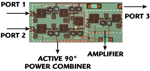
Figure 2 Photograph of the fabricated active 90° power combiner.
Figure 2 shows a photograph of the active 90° power combiner MMIC employing CE and CC InGaP/GaAs HBTs, which was fabricated on a GaAs substrate. The size of the fabricated chip, including the active 90° power combiner and amplifier, is 2.42 ×1.05 mm, which is 2.2 percent of the size of a conventional branch-line coupler fabricated on a GaAs MMIC (as mentioned previously, the size of a passive coupler is 10.54 × 10.92 mm).

Figure 3 Measured S31 and S32 characteristics.

Figure 4 Measured phase difference between S31 and S32.

Figure 5 Measured isolation characteristics.
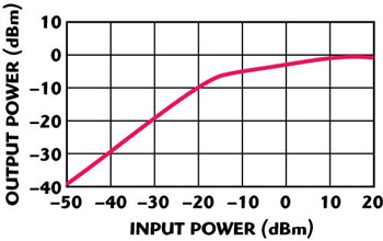
Figure 6 Output power characteristics.
Figure 3 shows the output gain characteristics (S31 and S32) of the active 90° power combiner. As shown, an equal output gain characteristic is observed from 2.3 to 2.5 GHz. Specifically, the proposed active 90° power combiner shows a gain of 10 ± 1 dB from 2.3 to 2.5 GHz due to the amplifier integrated on the MMIC. Figure 4 shows the phase difference characteristic of the active 90° power combiner. A phase difference characteristic of -90 ± 2.5° is observed from 2.3 to 2.5 GHz. Figure 5 shows the isolation characteristic between ports 1 and 2 of the active 90° power combiner. As shown, an isolation better than -25 dB is observed from 2.3 to 2.5 GHz. Figure 6 shows the output power characteristic of the active 90° power combiner. As shown, P1dB is approximately -3 dBm. The active 90° power combiner shows a power saturation level higher than -3 dBm due to the nonlinear characteristic of the InGaP/GaAs HBT. Therefore, the proposed active 90° power combiner can be used for a receiver or medium power transmitter of a wireless communication system. The characteristics of the active 90° power combiner are summarized in Table 1 for a comparison with the characteristics of a conventional 90° passive coupler.

Conclusion
In this work, a highly miniaturized active 90° power combiner employing CE and CC with InGaP/GaAs HBT was fabricated on a GaAs substrate for MMIC applications. For a 90° phase difference and equal power coupling, a novel composite structure is proposed, employing CE and CC circuits. The size of the active 90° power combiner including amplifier is 2.42 1.05 mm, which is 2.2 percent of the size of a conventional passive coupler. The active 90° power combiner showed good RF performances, comparable to those of a conventional passive coupler at S-band, and also showed a gain, due to the amplifier integrated on a MMIC. This work is the first report known of a 90° power combiner employing active devices.
Acknowledgments
This work was financially supported by the Ministry of Knowledge Economy (MKE) and the Korea Industrial Technology Foundation (KOTEF) through the Human Resource Training Project for Strategic Technology. This research was also supported by MKE, under the ITRC (Information Technology Research Center) support program supervised by the IITA (Institute for Information Technology Advancement), (IITA-2009-C1090-0903-0007) and the Korean Ministry of Education, Science and Technology Grant (The Regional Core Research Program/Institute of Logistics Information Technology), and also partly supported by KETI (Korea Electronics Technology Institute). This research was supported by MKE, Korea, under the ITRC support program supervised by the IITA (IITA-2008-C1090-0804-0007) and supported by DAPA and ADD under contract UD070054AD. This work was also partly supported by ETRI SoC Industry Promotion Center, Human Resource Development Project for IT SoC Architect.
References
1. S.A. Mass, Microwave Mixers, Artech House Inc., Norwood, MA, 1986.
2. T. Sugiura, K. Honjo and T. Tsuji, “12 GHz Band GaAs Dual-gate MESFET Monolithic Mixers,” IEEE Transactions on Microwave Theory and Techniques, Vol. 33, No. 2, February 1985, pp. 105-110.
3. E. Camargo and W. Kennan, “An E-mode GaAs FET Operating as a Single Balanced Gate Mixer,” 1996 IEEE MTT-S International Microwave Symposium Digest, Vol. 2, pp. 951-954.
4. K. Hubbard, K. MacGowan, C. Kau, D. Smith and S. Mass, “A Family of Low Cost High Performance HEMT MMICs for Commercial DBS Application,” 1995 IEEE Microwave and Millimeter Wave Monolithic Cicuits Symposium Digest, Vol. 1, pp. 133-136.
4. T. Kaneko, T. Miya and S. Yoshida, “A Ku-band Converter IC,” 1992 IEEE MTT-S International Microwave Symposium Digest, Vol. 1, pp. 451-454.
5. M. Chongcheawchamnan, G.N. Siripon and I.D. Robertson, “Design and Performance of Improved Lumped-distributed Wilkinson Divider Topology,” Electronics Letters, Vol. 37, 2001, pp. 501-503.
6. A.S. Sedra and K.C. Smith, Microelectronic Circuits, Oxford University Press, 2004.
Young-Bae Park received his BS and MS degrees in radio science and engineering from Korea Maritime University in 2005 and 2007, respectively. He is currently working toward his PhD degree at Korea Maritime University.
Young Yun received his BS degree in electronic engineering from Yonsei University, Seoul, Korea, in 1993, his MS degree in electrical and electronic engineering from Pohang University of Science and Technology, Pohang, Korea, in 1995, and his PhD degree in electrical engineering from Osaka University, Osaka, Japan, in 1999. From 1999 to 2003, he worked as an engineer with Matsushita Electric Industrial Co. Ltd., Osaka, Japan, where he was engaged in the research and development of MMICs for wireless communications. In 2003, he joined the department of radio science and engineering, Korea Maritime University, Busan, Korea. He is currently an assistant professor and his research interests include design and measurements of RF/microwave and millimeter-wave ICs and design and fabrication of HEMTs and HBTs.
In-Ho Kang received his PhD degree from Sogang University, Seoul, Korea, in 1995. He is now a professor in the division of radio and information communication engineering at Korea Maritime University, Busan, South Korea. His research interests include LTCC filters and MMIC filters for the RF single chip of 5.5 GHz WLAN, WiMAX and UWB applications, including MMIC filters for power amplifier harmonics suppression.
Ji-Won Jung received his BS, MS and PhD degrees in electronics engineering from Sungkyunkwan University, Seoul, Korea, in 1989, 1991 and 1995, respectively. Since 1996, he has been with the department of radio science and engineering, Korea Maritime University, Busan, Korea. His research interests include channel coding, digital modems, FPGA design technology and digital broadcasting systems.
Kwang-Ho Ahn received his BS degree in electronic engineering from Kyungpook National University, Daegu, Korea, in 1995, and his MS and PhD degrees in electrical and electronic engineering from Pohang University of Science and Technology, Pohang, Korea, in 1997 and 2001, respectively. From 2001 to 2006, he worked as a senior engineer at Samsung Electronics, Korea, where he was engaged in the research and development of radio frequency ICs (RFIC) for CDMA and WCDMA. In 2006, he joined the department of wireless components and telecommunications research center, Korea Electronics Technology Institute (KETI), Korea. He is now a managerial researcher and his research interests include design and analysis of CMOS RF transceivers and SoCs for UWB, ZigBee, WLAN and high frequency radar applications.