
To keep up with the growing needs of business sectors such as telecommunications, automotive, domotics, medical, aerospace and defense, the performance requirements of RF and HF transistors and amplifiers are increasing sharply. These products need to be affordable, and they must be able to handle more complex information, consume less power and still remain reliable. As a consequence, the design and performance tests of such devices are not a trivial task: It is time consuming, and the number of parameters that need to be tuned and checked are increasing exponentially. Several test and measurement manufacturers are vying for a share of this market. Indeed, there is a growing need for extensive RF and HF characterization capabilities of components operating under realistic conditions. Furthermore, the price must be affordable, even in situations where the S-parameters fail to do their job.
“Quid pro quo?”
Starting from regular DC and S-parameters, this article introduces more advanced applications by gradually extending commercially available vector network analyzers (VNA). The objective of these applications is to fully characterize active components, from small-signal to large-signal behavior under realistic excitations in a single connection. The article answers the questions, “Which nonlinear extensions should I buy first on my limited budget so that I can add more nonlinear capabilities when additional budget becomes available?” and “What do I gain with these extensions?”
From DC and S-parameters to complete large-signal characterization
DC Characterization
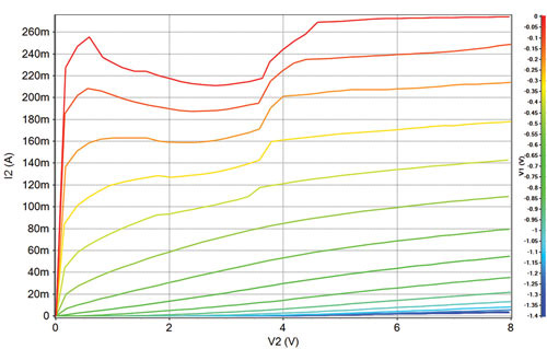
Figure 1 DC IV output characteristics.
When characterizing active components, a DC source is typically used to bias the device under test (DUT). This allows one to characterize the behavior of the device by performing a DC voltage/current sweep at the device’s input and output and by measuring the corresponding DC voltage-current relationship (see Figure 1). If necessary, calibration techniques can be applied to compensate for the losses of the bias tees and other cabling.
Small-signal Characterization

Figure 2 S-parameters vs. frequency.
Next, one can analyze the dynamic linear behavior of the component using small-signal characterization techniques. The S-parameters provide a uniform approach for adequately describing the linear behavior, relating the incident and reflected waves at both ports of the device. Today, vector network analyzers are commonly used instruments for performing small-signal measurements and for extracting the S-parameters at both ports of the device under test, as illustrated in Figure 2.
When designing a linear HF system, it is possible to use S-parameters as a model in combination with circuit-level models and tune certain parameters to achieve the design goal. Once the circuit is manufactured, it is measured using a VNA. The VNA provides S-parameters, which can easily be compared to simulation results. The loop from characterization, modeling, design and testing is closed using the same equipment. This avoids any discussions that may arise due to different equipment being utilized, as the vector network analyzer is used to share information across the complete cycle.
Enhancement of VNA with nonlinear capabilities
Triggered by the growing need for better insight into the nonlinear behavior of components, VNA manufacturers are adding various “nonlinear” features to some of their VNA models. These competitive features include AM-to-AM, AM-to-PM, harmonic power measurements and mixer characterization.1 Unfortunately, these features characterize the nonlinear behavior only partially as one essential piece of information is missing: The phase relationship between the different spectral components.
Indeed, mixer-based network analyzers do not allow one to measure the phase relationship between different tones. One frequency is measured at a time, and while stepping or sweeping the internal local oscillator from one frequency to the next, an arbitrary phase is introduced. In fact, the network analyzer is missing a phase reference in order to consistently capture the phase relationship between different tones.2,3

Figure 3 The NMDG ZVxPlus add-on kit on top of the R&S ZVA24..
Starting with commercially available network analyzers with the appropriate options (four-port, frequency offset measurement capability and direct access to the receivers), different extension kits exist, transforming the VNA into a mixer-based large-signal network analyzer (LSNA) and allowing complete harmonic characterization of active high-frequency components. Figure 3 shows such an example, combining a four-port R&S ZVA24 with the corresponding NMDG ZVxPlus add-on kit.
These extension kits include a synchronizer to add the missing phase reference to the VNA. The synchronizer is a very stable periodic pulse generator that generates a comb of harmonically related spectral components, which have a fixed phase relationship, in the frequency domain.
Four receivers of the VNA simultaneously capture a given harmonic of the incident and reflected waves at the input and output ports of the DUT, and—at the same time—a fifth receiver is used to measure the corresponding harmonic of the synchronizer. You can then reference the phase of the different harmonics at the DUT level to the phase of the corresponding harmonics of the synchronizer. Based on the fixed phase relationship of the output signal of the synchronizer, although not yet calibrated, the phase of all signals at the DUT level can be measured in a consistent way.
To eliminate the systematic errors of the measurement system, proper calibration techniques must be applied. In addition to a standard VNA calibration, two further calibration steps are required for accurate large-signal behavior analysis. First, a power calibration using a power meter is performed at fundamental and harmonics to take into account the amplitude distortion of the system. Next, the add-on kit includes an additional calibration element—a harmonic phase reference (HPR). This unique device enables the broadband harmonic phase calibration of the system and deals with the phase distortion of the measurement system.
Using de-embedding of extrinsic parasitics such as package or launcher pads, measurements close to the intrinsic nonlinearities of the device can be performed. The complete spectrum—in amplitude and phase—of incident and reflected waves, both at fundamental and harmonics, can then be acquired and the time waveforms reconstructed.
Large-signal characterization
Small-signal network analysis implies that the signal levels are sufficiently small such that the device behaves linearly. Many applications today require signal levels that are significantly higher, driving the RF ICs in their nonlinear region of operation. Even more difficult, transistors are driven in a highly nonlinear manner to transmit signals with high efficiency but low distortion.
At this stage, S-parameters are no longer adequate and there is a need to “go beyond S-parameters.” Indeed, as soon as the device behaves nonlinearly, the superposition principle is no longer valid. Therefore, it is crucial to be able to put the DUT under realistic large-signal operating conditions and to acquire complete and accurate information about its electrical behavior for different classes of signals.
Possible candidates are either voltage and current or incident and reflected waves. Depending on the application, one will use the representation that provides the best insight. For example, process engineers and transistor modelers tend to use the voltage and current formalism, while system engineers generally prefer the wave quantities.
Moreover, signals can be visualized both in the time and frequency domain. Again, process and transistor modeling engineers tend to prefer the time domain because their models are formulated in that domain, while system engineers prefer the frequency domain, as the system level specifications such as adjacent channel power ratio (ACPR) or spectral re-growth are expressed in this domain. All these different data representations and visualizations are possible with a mixer-based LSNA.
Continuous waves characterization close to 50 Ω environment
Now assume that one wants to characterize the large-signal HF behavior of a biased FET transistor, using a continuous wave (CW) excitation (for example at 2 GHz) at the gate, and terminated close to 50 Ω at the drain. If the device is stable (not oscillating) and does not exhibit sub-harmonic or chaotic behavior, all currents and voltages (or wave quantities) will have the same periodicity as the drive signal (in this case 0.5 ns).
Presently, large-signal network analysis is limited to CW or periodic modulated signals where the fundamental carrier and fundamental modulation frequency do not have to be commensurate. Like a spectrum analyzer, the LSNA allows you to visualize the spectral data of the measured quantities in the frequency domain. The unique feature here is that the spectral data includes calibrated phase information (see Figure 4).

Figure 4 Incident (a) and transmitted (b) wave quantities in the frequency domain.
An oscilloscope is an indispensable tool on the lab bench for probing signals and for checking the proper behavior of circuits. Today, sampling scopes with a real-time bandwidth higher than 10 GHz are available. However, voltage information alone is not enough, and one needs to add a proper test set and calibration techniques to accurately measure the component behavior. The advantages of using vector network analyzers instead of oscilloscopes have clearly been proven for linear RF and HF applications.

Figure 5 Input and output voltages and currents in the time domain for small-signal (a) and large-signal (b) conditions.
The LSNA can provide the voltage and current waveforms at the input and output ports of a device under test, as illustrated in Figure 5 under both small- and large-signal conditions. When the input power is low, one can observe sine waves for all quantities. For high input power—due to nonlinear behavior of the device—one will start to observe distortion of the waveforms such as the clipping effect of the output current.

Figure 6 Dynamic source (a), transfer (b), and load (c) lines on top of DC voltage-current characteristics.
Using the above voltage and current waveforms in the time domain, one can display the dynamic trajectories:
- Dynamic source line, i.e. i1(t) as function of v1(t) (see Figure 6a)
- Dynamic transfer line or dynamic gm, i.e. i2(t) as function of v1(t) (see Figure 6b)
- Dynamic load line, i.e. i2(t) as function of v2(t) (see Figure 6c)
Furthermore, as both quantities at the input and output of the device are measured simultaneously, the mixer-based LSNA allows one to map the dynamic excursion of the input voltage v1(t) to the static input voltage using, for example, gradient colors as a 3rd dimension, resulting in a 3D dynamic load line. If the color of the input voltage v1(t) does not match that of the DC input voltage, it indicates that the measurements do not correspond to the intrinsic static nonlinear behavior of the component and that other phenomena are present, such as delay between input and output or trapping and memory effects.

Figure 7 Fundamental, second and third harmonic impedances presented at the device output.
Using the basic information, one can also calculate the input reflection coefficient of the device and the load reflection coefficient, presented at the output of the device, both at fundamental and harmonics. Typically, these quantities are visualized using a Smith Chart (see Figure 7).
Characterization in a non-50 Ω environment
Today, power amplifier (PA) designers mainly use load-pull systems to extract specifications such as output power or power added efficiency (PAE) under different source and load impedance conditions. Such a system, based on passive (mechanical or electrical) or active (active loop or injection of power using an external source) tuning, has several drawbacks: Preparing the setup with the tuners is time-consuming and cumbersome, while the tuning process is slow due to the power meters which are typically used and the precise movement of the passive tuners. Furthermore, the broadband power measurements do not differentiate between fundamental and harmonics. As a result, one cannot be sure that the amplifier is being used exactly in the desired class of operation.
While the calibration of a classic load-pull system4 requires off-line characterization of all parts of the measurement setup, one can (re)-configure the stimuli at the input and output of the LSNA without recalibration. One can then study the DUT behavior under realistic conditions with a single device connection and without the need to calibrate the tuner. For highly mismatched components, this setup is not adequate because the couplers used to capture incident and reflected waves are lossy components and they will degrade the tuner performance in terms of highest possible gamma presented to the DUT. One solution is to put the tuner between the DUT and the couplers. However, changing the tuner position invalidates the calibration, and one still needs to characterize the tuners separately and use an S-parameter-based de-embedding technique for each tuner position.
Another issue appears as soon as one wants to perform harmonic tuning using a passive tuner. Indeed, since one generally wants to present a high reflection coefficient for the harmonics, most if not all of the harmonic energy will be reflected back to the DUT before reaching the reflectometers. As such, the VNA will not be able to accurately measure the harmonic behavior.
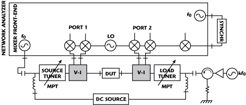
Figure 8 Device characterization in non-50 Ω conditions: combining LSNA with harmonic tuners and new probing solutions.
In recent years, research has focused on overcoming these various drawbacks.5 New probing solutions were introduced for harmonic tuning using a quasi-lossless coupler-like structure to be inserted between the DUT port and the tuner hardware. If one combines the LSNA with this new probing solution and a multi-harmonic tuner6 (see Figure 8), one can accurately characterize the component in a harmonic non-50 Ω environment while controlling independently the fundamental up to the 3rd harmonic impedances presented at both its input and output port.
Characterization under pulse and modulation conditions
Using the pulse capability of some VNAs such as the R&S ZVA, the nonlinear extension kits can be used to perform these large-signal measurements under pulsed conditions, both in average pulse and pulse profile mode. Combined with pulsed DC equipment, one can then extract the nonlinear behavior of the component while avoiding contributions of heating and trapping effects. Moreover, due to the large IF bandwidth of the R&S ZVA, large-signal measurements under modulation conditions can be performed efficiently by capturing the full IF bandwidth around each harmonic.7
Design
Improvement of Large-signal Transistor Models
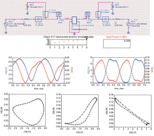
Figure 9 Model verification using large-signal measurements.
One should notice that the voltage and current quantities contain both the amplitude and phase information at fundamental and harmonics. This is essential for process and transistor modeling engineers as these quantities are directly usable in the harmonic-balance simulation tools. Using the mixer-based LSNA, model verification in 50 Ω conditions can already be performed by using the measured voltages at the input and output ports of the device as stimuli in the simulation and comparing the measured currents to the simulated ones. A more realistic model verification can also be done in non-50 Ω conditions by combining LSNA with one of the tuning techniques. In both cases, one can be sure that they tested the model under the same realistic conditions as during the measurement of the “real” component (see Figure 9).
Power Amplifier Design Made Easy

Figure 10 Setup combining R&S ZVA24 with Focus V-I Probes and MPT multi-harmonic tuner.
When you combine the LSNA with new quasi-lossless probing solution and multi-harmonic tuning techniques (see Figure 10), the design of an amplifier in the desired class of operation using waveform engineering becomes almost as easy as in the theoretical textbooks.8 Indeed, amplifier designers can now on-the-fly visualize the dynamic load line and voltage and current waveforms as close as possible to the intrinsic level of the amplifier. They can also monitor different figures of merit such as output delivered power or PAE, while controlling independently the fundamental up to 3rd harmonic impedances presented to the device output.

Figure 11 Visualizations of a high-efficiency heterojunction power FET device optimized in class B: output voltage waveform (a), output current waveform (b), dynamic load line (c) and fundamental up to 3rd harmonic impedances presented at output of the device (d).
Using this unique measurement solution, excellent agreements with theoretical performance have been observed on a commercially available high-efficiency heterojunction power FET9 by optimizing fundamental and harmonic output impedances for different classes of operation. Figure 11 shows the measurement results with the device optimized for class B. The optimization only took a couple of minutes, and the obtained PAE of 74 percent is very close to the theoretical PAE of 78.5 percent.
Behavioral Modeling
The S-parameters can be regarded as a measurement-based small-signal behavioral model of the DUT. Moreover, the small-signal network analysis is independent of the type of component and independent of the process technology. This explains the success of S-parameters for passive or active components used in their linear mode of operation.
Unfortunately, there is as yet no such uniform approach for dealing with nonlinear RF and microwave problems. One can deal with a subset of these phenomena in a uniform way using existing modeling techniques such as the describing functions introduced in the late ‘90s,10 a natural extension of S-parameters to model the nonlinear behavior of active components.11 To extract a small-signal behavioral model, the S-parameters can be measured at different DC bias points. One should notice that while they correctly describe the small-signal behavior of the component at each of these DC bias points, the S-parameters themselves become a nonlinear function of the DC operating points.
Under large-signal conditions, the above DC-bias-dependent S-parameters do not correctly describe the behavior of the component. To describe the nonlinear behavior of the component, an additional “bias” point is required: The large-signal input tone. Because the component is driven by this large-signal input tone, the reflected and transmitted waves will also contain harmonics. Considering both the DC bias and fundamental tone as part of the large-signal operating point (LSOP), one can already describe the nonlinear relationship between incident and reflected waves at both the input and output port of the device. In addition, one can measure the “S-parameters” as a function of frequency by performing a forward and reverse measurement. Beyond the fundamental and harmonics at k.f0 resulting from the large-signal input tone and the small-signal input tone at frequency f, additional tones will show up at k.f0 ± f. A linear relationship does exist between the small-signal input tone and the resulting output tones. This linear relationship also depends on the large-signal operating point and describes the behavior of the component due to perturbations on top of the large-signal input tone. The combination of both the nonlinear and linear relationships is referred to as S-functions instead of S-parameters because of their dependency on the LSOP.11
 (a)
(a)
 (b)
(b)
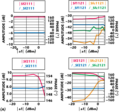
Figure 12 S-functions extraction setup (a) and corresponding block diagram (b).
 (a)
(a)
 (b)
(b)
Figure 13 S-functions visualization (a) and verifications using an independent set of measurements (b): The measured DC (red), fundamental (green), second (blue) and third (purple) harmonic spectral components of the transmitted wave b2 are shown. Black dots: amplitude in dB of complex difference between measured and predicted b2.
When applying the large-signal tone using an external source, the LSNA can be reconfigured to extract the S-functions using the internal source of the VNA to apply the small-signal input tone at the fundamental and at harmonics k.f0 either at the input or output of the DUT (see Figures 12 and 13). One can also use the different tuning techniques to extract the S-functions in non-50 Ω conditions. Like the S-parameters, S-functions can be cascaded. Imported in CAE tools, S-functions can then predict both harmonic and modulation behavior, under quasi-static assumption, from the component level up to the system level under non-50 Ω conditions in a uniform manner.
Conclusion
If one wishes to extend the capabilities of network analyzers at an affordable price, add-on kits are available to provide unique insight into the behavior of active components. By setting up a single connection, engineers can now visualize the linear and nonlinear behavior of their components and also verify and certify their models against large-signal network analysis techniques.
Combining this unique large-signal measurement solution with the latest tuning technologies, it is now possible to match transistors at both fundamental and harmonics to optimize their performance based on instantaneous feedback provided by the voltage and current waveform measurements. By extracting measurement-based behavioral models via the S-functions, engineers can improve and speed up their design process by measuring and directly simulating RF systems under large-signal conditions. Manufacturers can also provide more complete system-level models of their RF devices. Starting with a set of commercially available vector network analyzers, one can gradually add nonlinear measurement and modeling capabilities under realistic conditions, including fundamental and harmonic mismatch. This approach will surely open new frontiers.
References
1. Rohde & Schwarz, “R&S ZVA Vector Network Analyzer,” Product Brochure, www.rohde-schwarz.com.
2. U. Lott, “Measurement of Magnitude and Phase of Harmonics Generated in Nonlinear Microwave Two-ports,” IEEE Transaction on Microwave Theory and Techniques, Vol. 37, No. 10, October 1989, pp. 1506-1511.
3. D. Barataud, et al., “Measurements of Time Domain Voltage/Current Waveforms at RF and Microwave Frequencies, Based on the Use of a Vector Network Analyzer, for the Characterization of Nonlinear Devices, Application to High Efficiency Power Amplifiers and Frequency Multipliers Optimization,” IEEE Transactions on Instrumentation and Measurement, Vol. 47, No. 5, October 1998, pp. 1259-1264.
4. Focus Microwaves, “Basics on Load Pull and Noise Measurements,” Application Note AN-8, www.focus-microwaves.com.
5. J. Verspecht, “Advanced Measurements for Characterizing Power Transistors,” 2007 IEEE Topical Symposium on Power Amplifiers for Wireless Communications, Invited Talk.
6. Focus Microwaves, “MPT, a Multi-Purpose, Vibration-Free Tuner,” Product Note PN-79, www.focus-microwaves.com.
7. M. Vanden Bossche, “Technology Update on Nonlinear Capabilities with Vectorial Network Analyzers,” ARFTG NVNA User’s Forum, Boston, MA, June 2009.
8. S.C. Cripps, RF Power Amplifiers for Wireless Communications, Second Edition, Artech House Inc., Norwood, MA 2006.
9. Excelics EPA120B Datasheet, www.excelics.com.
10. J. Verspecht and P. Van Esch, “Accurately Characterizating of Hard Nonlinear Behaviour of Microwave Components by the Nonlinear Network Measurement System: Introducing the Nonlinear Scattering Function,” Proc. International Workshop on Integrated Nonlinear Microwave and Millimiter-wave Circuits (INMMiC), October 1998, pp. 17-26.
11. NMDG NV, “S-functions—Measure, Model, Simulate—An Application in ICE,” presentation, www.nmdg.be.