
Power amplifiers (PA) are a critical functional block in today's wireless communications. They are found in every cell phone, cordless phone, RF remote controller, etc. Any application requiring the wireless transmission of analog or digital signals will require a PA. In wireless equipment, the PAs are usually placed as close as possible to the antenna to minimize RF losses, maximize power efficiency and maximize battery life. RF systems engineers need to determine the PA return loss under actual output power drive levels. This so-called "Hot S22" is needed to calculate the mismatch loss at the antenna interface and to determine the actual wireless system transmit power (a key requirement for regulatory bodies, such as the FCC).
The verification of a PA output return loss has proven to be a problematic and challenging endeavor when the PA is delivering high output power. High power PAs will inadvertently heat up as the output power levels are increased. Under high output power conditions, the power transistor's parameters may significantly change as temperature and bias conditions change.1 Therefore, the PA output return loss may be substantially different when operated under low output power versus high output power. Most PA suppliers will only publish return loss values under small-signal conditions. These values should be checked against actual high power conditions when conducting systems transmit power budgets. A number of test equipment suppliers have "off-the-shelf" test hardware for measuring the return loss of high power units,2,3 but these solutions are usually very expensive, and may not justify the investment for engineers conducting only occasional high power tests.
This article outlines a simple and cost-effective solution for determining the return loss of a high power PA. A test procedure is outlined, based on a mathematical approach, to determine the PA large- (or small-) signal return loss by measuring the insertion phase variation of the PA at specific VSWRs, using an inexpensive and simple test arrangement.
PA Reflection Coefficient
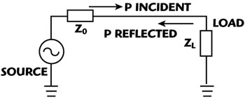
Figure 1 Power transmission from source to load.
Any RF test configuration can be expressed by a source impedance ZL, and a characteristic impedance (Z0), as shown in Figure 1. If the load impedance is equal to the source characteristic impedance then the reflected traveling wave does not exist (as is the case for a matched load). However, when ZL is not equal to the PA output impedance Z0, then the traveling wave V between the PA to the load contains two components: one is traveling in the +z direction and the other traveling in the -z direction.

The traveling wave in the +z direction is the incident power, and the traveling wave on the -z direction is the reflected power.


where γ is the propagation constant.

Figure 2 PA in a mismatch system.
Now replace the source with an actual PA and the load with a phase tuner, which rotates the phase by 2π radians and causes, in theory, full reflection back to the PA, as illustrated in Figure 2. The reflection coefficient is determined to be the ratio between the reflected and the incident vector as follows:

where:
Φ is the shifted phase caused by the PA
θ is the phase angle of the reflection coefficient ΓL
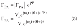
Ψ is the phase angle of the reflection coefficient ΓPA
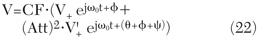
The summing vector, V, in the coupled port contains three vectors that are directed from three different paths, that is:


where CF is the bidirectional coupling factor and DR is the directivity for the bidirectional coupler.


Using directional couplers with DR > 20 dB, ensures that V3 is much smaller than V2, that is:
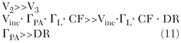
It is recommended that the directivity for the bidirectional coupler should be higher than the PA return loss by 15 dB. This will ensure that the vector V3 will remain negligible.
Directivity ≥ PA R.L + 15 dB
If V3 is negligible, then the vector V can be reduced to:


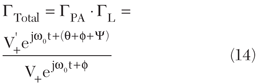


Figure 3 The reflected wave vector is rotating 2π radians across the incident wave vector.
The summing vector V, as illustrated in Figure 3, contains the vector V1, which represents the incident wave and the vector V2, which represents the reflected wave.
The angle φ is the angle between the incident vector V1 to the summing vector V and is also determined as the variation in PA insertion phase between the PA insertion phase at VSWR=1:1 to the PA insertion phase when the phase tuner is shifted within 2π radians with VSWR>1.

Figure 4 Vector diagram for maximum and minimum insertion.
There are two locations on the phase tuner where the maximum and minimum PA insertion phase is achieved. At these two locations, the reflected vector is perpendicular to the incident vector and the angle reaches the highest value, φMAX, as shown in Figure 4. At these two locations of 90° insertion phase, the product of the load and PA reflection coefficients can be written as:

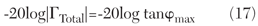
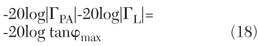

Since the phase tuner has a full reflection then ΓL = 1 and the PA return loss (in dB) can be expressed as:

φMAX can be found by rotating the phase tuner within 2π radians and the maximum insertion phase can be searched using a phase detector with the test setup shown in Figure 5.

Figure 5 Test setup for measuring maximum insertion phase.
PA Reflection Coefficient with a Determined Mismatch Load
In practice, PAs are specified over a limited VSWR range. The PA can be damaged or unstable with a load VSWR above what has been specified by the vendor.

Figure 6 Test setup for measuring maximum insertion phase with limited VSWR.
Therefore, the same analysis will be given when the load phase tuner is connected to the PA through an attenuator in order to limit the VSWR that will reflect on the PA (see Figure 6).


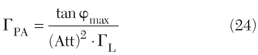

Since the phase tuner has a full reflection, ΓL = 1, the PA return loss can be expressed as:

or

If the PA return loss is high and the attenuator used between the PA to the phase tuner is high, then the phase angle φMAX may be small and difficult to measure in order to have accurate results. Therefore, it is suggested to use a small attenuator (1 to 3 dB) between the PA and the phase tuner.
Test Method

Figure 7 Test setup for matched load.
Step 1:
Connect the PA as illustrated in Figure 7 using a 50 Ω load at the output of a bidirectional coupler (additional attenuation can be connected in front of the phase detector whenever it is desired to measure the return loss for a very high power PA).
Measure the insertion phase at the various frequencies of interest using small-signal or large-signal input power. The insertion phase with a 50 Ω load will be the reference insertion phase before loading the PA with different VSWRs.

In Table 1, the measured value for a high power (2 W), 350 to 470 MHz, Skyworks' PA (SKY65141), is shown.

Figure 8 Test setup for mismatched load.
Step 2:
Disconnect the 50 Ω load at the output of the bidirectional coupler and connect a 1.5 dB pad in order to present the PA with a VSWR = 6. Place a phase tuner after the fixed attenuator pad. The phase tuner must be capable of continuously varying the insertion phase from 0 to 360°. The test setup is illustrated in Figure 8. Adjust the phase tuner in order to find the highest and lowest insertion phase and calculate at each frequency what the maximum phase variation is, compared to the insertion phase at 50 Ω, as indicated in Table 2. Note that the attenuator value is selected to be within the specified PA load VSWR range. The total output insertion loss should be measured at each maximum insertion phase location on the phase tuner in order for the return loss to be calculated accurately.

In theory φMAX = φMIN , therefore the following equation is valid:
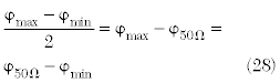
However, in practice φMAX and φMIN may not be equal since the phase tuner may not be ideal and symmetric. Therefore, the insertion phase at VSWR = 1 (φ50Ω) is subtracted from the absolute value for the maximum phase variation (φ-φMAX or φ+φMAX).
The return loss of the PA is calculated according to the following formula:

where θMAX is in degrees and Att is the measured attenuation from the PA output to the phase tuner input.
Test Results

Figure 9 Return loss measured at low power.
The theoretical analysis shown in the above sections was verified using a high power 2 W SMT PA from Skyworks (SKY65141). The PA was tested over its entire operating frequency range, 350 to 470 MHz. The actual return loss measurement was made with a network analyzer at small input signal and the results are given in Figure 9.
The measurement results are compared to the calculated return loss using the proposed phase measurement procedures outlined in the above sections.

Figure 10 Calculated PA return loss at Pin - -30 dBm.

Figure 11 Calculated return loss Pin = -4 dBm and VSWR = 3.5.
The new test procedure was done using different load VSWRs to demonstrate that the return loss measurements are repeatable at different VSWRs. The return loss obtained using the new proposed phase technique is shown in Figures 10 and 11. The same method was used to calculate the PA return loss using higher input signal with VSWR = 3.5. A photo of the PA mounted in its test fixture is shown in Figure 12.

Figure 12 Photo of high power PA (SKY65141) mounted in its test fixture.
Conclusion
A PA return loss is a parameter, which can vary depending on the PA output power, the PA bias current, etc. Therefore, the PA return loss under high output power conditions should be measured and not be assumed to be the same as the return loss measured under small-signal output power conditions. The PA return loss can be calculated from the phase between the summing (incident and reflected vectors) to the incident vector, which is measured with a matched-load.
This article demonstrates that the "hot" PA return loss can be accurately calculated by measuring the maximum insertion phase variation at any given VSWR, and at any given input drive level. The proposed return loss measurement technique can be implemented using low cost test components, eliminating the need for costly network analyzers.
References
1. L. Liou, J. Ebel and C. Huang, "Thermal Effects on the Characteristics of AlGaAs/GaAs Heterojunction Bipolar Transistors Using Two-dimensional Numerical Simulation," IEEE Transactions on Electron Devices, Vol. 40, No. 1, January 1993, pp. 35-40.
2. "Recommendations for Testing High-power Amplifiers," Agilent Application Note 1408-10.
3. "Hot S22 and Hot K-factor Measurements," Anritsu Application Note AN11410-00295.