
The design of either a power amplifier, low noise amplifier, narrow band amplifier or wideband amplifier has been a challenging task for the microwave engineer. Stability is the most important issue the engineer has to face.1 It can haunt a designer, starting from the design phase, through the selection of active and passive components, assembly and product verification, all the way to the final delivery.
The theory behind stability, however, is simple1,2 — the amplifier must operate with a stability factor greater than one, and the reflection coefficients of the input and output matching networks must stay outside the unstable region of the active devices. To prevent the oscillations from happening, many engineers use a trial and error method. This is effective, but quite time-consuming, and experience plays a very important role.
A study of stability of a two-stage wideband amplifier was performed. Figure 1 is the block diagram of the wideband amplifier under investigation. It consists of two packaged amplifiers connected through bonding wires, three DC blocking capacitors and an SMA connector at the input and output ports. Each amplifier stage has free oscillations at 11.3 and 12.0 GHz, respectively. The two-stage amplifier oscillates at 11.5 GHz if it is built as illustrated in the diagram. Aside from the experimental method, a 3D electromagnetic (EM) solver and electronic design automation (EDA) software were relied upon to find a feasible solution to the oscillation problem.

Fig. 1 Block diagram of a two-stage amplifier.
There are currently a number of commercially available full-wave solvers and circuit simulators. The High Frequency Structure Simulator (HFSS) from Ansoft and the Agilent EEsof Advanced Design System (ADS) are employed for this study. First, the SMA connector and wirebond interconnect are modeled using HFSS. The S-parameters of the two single-stage amplifiers are obtained through probing measurements. The errors in the measurements are corrected through HFSS modeling of the probe transitions. Circuit simulations are then performed with ADS to examine and analyze the S-parameters and stability regions of the amplifier. In the end, the simulations reveal that an inductor of value greater than 0.5 nH between two single-stage amplifiers can achieve the overall stability. Statistical analysis in ADS is also conducted to examine the sensitivity of the inductor to manufacturing variations. An Anritsu 37347C vector network analyzer (VNA) is utilized to take all S-parameter measurements.
EM Modeling and Circuit Simulations
The SMA and the wirebond transitions are modeled using HFSS and the responses are exported to ADS for circuit simulations. Figures 2 and 3 show the modeled SMA and wirebond transitions.
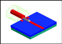
Fig. 2 3D model of the SMA transition.
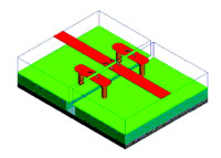
Fig. 3 3D model of the wirebond transition.
The VNA is calibrated using a commercial calibration kit, in which the standards have a different geometry from that of the ground-signal-ground (GSG) structure on the package substrates of the single-stage amplifiers. The errors caused by the discrepancy must be corrected before the measured data are post-processed in the circuit simulations.3,4 Figures 4 and 5 show the modeled probe transitions on the calibration substrate and on the substrates of the amplifier, respectively. Based on the two simulations, the errors in the measurements can be easily subtracted.

Fig. 4 The modeled probe transition on the commercial calibration substrate.

Fig. 5 The modeled probe transition on the package sunstrate.
In ADS, the simulation shows that the two-stage amplifier oscillates at 11.5 GHz, which correlates very well with the measurement. To suppress the oscillation, the topology of the inter-stage matching network may have to be reconfigured.1 The stability of each stage amplifier is explored through circuit simulations done in ADS to determine an optimal matching network.
The load stable region of the first-stage amplifier is examined at 11.3 GHz, including the impact of the connector (refer to the block diagram). The reflection coefficient, Gin, seen looking into the second stage, is also analyzed. Both results are plotted on a Smith chart with unity radius, as shown in Figure 6. It can be seen that Gin lies outside of the stable region. The plot also indicates that if a certain amount of inductance is introduced, Gin becomes inductive and can be moved into the stable region. More simulations show that a 0.5 nH inductance is the minimum required to achieve the stability.

Fig. 6 Load stability circle of the first-stage amplifier and the input reflection coefficient ?in of the second stage
The source stable region of the second-stage amplifier is analyzed at 12 GHz with the responses of the wirebond transition and SMA connector taken into account. The reflection coefficient, ?out, seen looking into the output of the first-stage amplifier, is simulated. The results are plotted on a Smith chart shown in Figure 7, which shows that ?out is located in the marginally stable region. However, any amount of inductance added to ?out will keep it to remain in the stable region. The analyzed results show that if an inductor of 0.5 nH or greater is inserted in the inter-stage network, the oscillation of the amplifier will be suppressed.

Fig. 7 Source stability circle of the second-stage amplifier and output reflection coefficient ?out of the first stage.
A 1.0 nH, wound-wire SMT inductor in a 0402 type casing is chosen for this study. It is mounted on the output microstrip line of the first-stage amplifier. The selected component is modeled through the use of HFSS to take the impacts of its parasitic capacitance into consideration. In ADS, the stability and S-parameters of the two-stage amplifier are re-examined. The simulations also point out the optimal location for the placement of the inductor.
To account for the tolerance in the inductance, an equivalent circuit is developed by fitting the responses with the ones obtained from HFSS modeling. The circuit and results are shown in Figure 8. Notice that the inductance in the equivalent circuit is right at 1.0 nH. Figure 9 displays the 3D model of the inductor. In ADS, a Monte Carlo analysis, with 500 trials, is performed with the assumption that the inductance and the capacitance vary ±10 percent of their nominal values. The constrains defined for the analysis are: the magnitude of S11 and S22 should be smaller than –10 dB, and the stability factor should be larger than unity. ADS shows a resulting yield of 95 percent within the bandwidth of interest.

Fig. 8 SMT inductor's (a) equivalent circuit, and (b) comparison between the equivalent circuit response and HFSS modeling.

Fig. 9 Modeled 0402 SMT wound-wire inductor.
Experimental Results
A couple of two-stage amplifiers were built, according to the results of the modeling and simulations described above. All the measured S11 and S22 magnitudes become smaller than unity at 11.5 GHz. Figure 10 displays the input reflection coefficients of a typical two-stage amplifier before and after the introduction of the stabilizing inductor. The effectiveness of the solution is quite obvious. Another measurement taken through a spectrum analyzer confirms that there is no free oscillation over the frequency band of interest.

Fig. 10 Measured S11 magnitude before and after introducing the stabilizing inductor.
Conclusion
The stability of a two-stage broadband amplifier is studied by means of circuit simulation in conjunction with EM modeling of the passive structures of the amplifier. The single-stage amplifiers are characterized utilizing probe measurements. The probing measurement errors are corrected through EM modeling as well. The analysis results in a solution to mitigate the oscillation problem of the amplifier. The effectiveness of the solution is verified by experiment. The accuracy of EM modeling and circuit simulation is demonstrated.
Acknowledgments
The author would like to acknowledge the support of the management of BreconRidge Manufacturing Solutions. Dr. Tibor Lapohos developed the macro to generate the complex 3D model of the GSG probe.
References
1. G.D. Vendelin, A.M. Pavio and U.L. Rohde, Microwave Circuit Design Using Linear and Nonlinear Techniques, John Wiley & Sons Inc., Hoboken, NJ, 1990, pp. 211–383.
2. D.M. Pozar, Microwave Engineering, John Wiley & Sons Inc., Hoboken, NJ, 1998, pp. 600–641.
3. D.K. Walker and D.F. Williams, “Compensation for Geometrical Variations in Coplanar Waveguide Probe-tip Calibration,” IEEE Microwave and Guided Wave Letters, Vol. 7, No. 4, April 1997, pp. 97–99.
4. G. Carchon, W.D. Raedt and E. Beyne, “Compensating Differences Between Measurement and Calibration Wafer in Probe-tip Calibrations,” 2002 IEEE MTT-S International Microwave Symposium Digest, Vol. 3, pp. 1837–1844.
Xiaoming Chen received his PhD degree in electrical engineering from the University of Electronic Science and Technology, China, in 1991. He worked with Nanjing Electronic Device Institute from 1991 to 1996, where he designed and developed GaAs MMICs and power MESFETs. He joined Gateway Technologies, Singapore, for the design of mixers and power amplifiers in 1996. Between September 1998 and June 1999, he conducted a post-doctoral study at Dalhousie University, Halifax, Canada, to develop patch antennas and analyze package resonances. From 1999 to 2003, he worked with Nortel Networks Inc., where he was involved in the design of packages and modules for 10/40 Gbps and millimeter-wave applications. In August 2003, due to the acquisition of the microelectronic group from Nortel, he joined BreconRidge Manufacturing Solutions, Ottawa, Canada. His primary interests include electronic component modeling, design of RF circuits, wireless and microwave communications systems, and measurement techniques.