
The advancement of CMOS technology over the past two decades has had a tremendous impact on shaping the semiconductor industry. It was reported in early 1984 that CMOS was finally starting to have a significant impact on the electronics field and was beginning to gain substantial market share.1 CMOS technology had lain dormant for several years prior, while PMOS and NMOS each had their day. With semiconductor tool capability reaching the 3 ?m technology node in the early ’80s, CMOS became a viable technology for moderate to high gate counts. Bipolar technology likewise continued to advance, but it came under severe competition once CMOS became a competitive commodity.
In a similar time period, gallium arsenide (GaAs) also revolutionized the lumbering RF/microwave market. GaAs MMICs brought integration capability to the predominately chip-and-wire-based military and high frequency markets. Numerous technical advances were made in the III-V compound semiconductors that painfully followed the integration and manufacturing achievements made in silicon (Si) technologies several years before.
Today there are a variety of Si- and GaAs-based technologies and a corresponding mix of bipolar and field effect devices that are routinely used to achieve optimized combinations of low cost, high performance, and minimum-sized solutions for wireless- and communication-based systems. Understanding the advantages and trade-offs of any particular technology is important in today’s market, yet it is far more important to be able to compare the benefits of one technology against those of several other technologies. The design engineer of today needs to be versed in several technologies and their specific devices in order to guide product development towards the best combination of technologies for a given solution in order to remain competitive. It is with this understanding and perspective that a review is presented of the past, the present and the future role of various semiconductor technologies used in wireless handsets.
RF Front-ends for Wireless Handsets
Significant attention is given to the configuration and specification of the RF front-end of wireless handsets with emphasis on the interconnect between the antenna and the transmit/receive chains (see Figure 1). The early analog handsets used a simple duplexer; however, as digital phones, with formats such as TDMA, became popular, the need for a low cost switch became evident. The early and popular choice was the use of PIN diode-based switches. A very popular solution for dual-band GSM radios incorporated low temperature co-fired ceramic (LTCC) modules, taking advantage of the passive filter and diplexer function built into the PIN-based switching module. Today multi-band multi-mode architecture and aggressive DC current budgets are forcing the PIN diode solution to either join or be replaced by GaAs-based or SOI (silicon on insulator) type structures.

Fig. 1 Wireless handset block diagram.
GaAs has enjoyed a strong place in the T/R, mode selection and antenna switching area. The very low dissipation and small size made it an ideal choice; the switching Q and ESD susceptibility, however, required novel circuit solutions to make it competitive.
SOI-based switches integrating the RF with the CMOS logic is beginning to show promise and could threaten the GaAs switch in some applications. A potential newcomer to this arena are micro-machined electro-mechanical (MEM) switches. Still in their infancy, they show promise with some outstanding performance features, particularly insertion loss.
The History of GaAs FET Switches
The early 1980s saw significant funding in the GaAs-based component arena. Most of the funding was directed at LNA and PA functions. However, some of the funding supported the development of T/R switching, which would be integrated with PAs or LNAs and form PA or LNA multifunction modules. The initial switch designs fell well short of the frequency bands for which they were intended. It became clear that the 2 to 18 GHz applications were going to incorporate more conventional switching techniques.
The GaAs FET switch, however, did have some significant features. The bias structure was a simple 10 kW resistor and the bandwidth was an incredible DC to 5 GHz (limited by the FET’s parasitic capacitance). In addition, it required voltage applied to the gate to actuate the switch. The only current drain was due to the leakage level of the FET, which was less than 50 mA. These features allowed the device an early acceptance in the IF bands of microwave circuits.
The 2 to 18 GHz Challenge
Most of the microwave switch applications focused on the military 2 to 18 GHz frequency ranges. The technology that dominated the market was PIN-based microstrip and stripline circuit switches. These switches were focused not only in the various bands such as L-band, S-band, etc., but also the entire 2 to 18 GHz range. To accomplish the kind of bandwidth required, PIN diodes needed to have cut-off frequencies (fc) in the 600 to 800 GHz range. (fc is defined as the frequency at which the off capacitance of the device is equal to the geometric mean of the off and on resistances.) Anything short of those values would be noncompliant to the specification demanded by the overall system requirement. This translated to performance being the key factor in winning the switch business. Although cost was very important, there would never be a “trade-off” of performance to achieve lower product cost.
When the first MESFET-based switches appeared, the performance was competitive with the PIN switch below 1 GHz. The typical fc for the MESFET device was approximately 125 GHz. By using novel circuit techniques, one could compete over narrow band applications, but in no way could the MESFET switch handle the octave bandwidths required above 2 GHz.
Disappointment Leads to Opportunity
The failure of the GaAs MESFET’s ability to compete in the 2 to 18 GHz range forced proponents of the device to look below the 2 GHz range. The IF bands provided the answer, but the requirements were different. Switch cost played a more significant role, and although performance was still the priority, it was easily achieved by lower Q diodes. This resulted in lower cost components using plug-in type packages, rather than expensive RF coax connector-based precision machine housings. The IF bands covered 2 to 500 MHz and here the MESFET excelled. The switch could easily handle the bandwidths and provided the opportunity to go well below 2 GHz; in fact, it could go all the way to DC. The limiting bandwidth factor was not fc but the range of the RF bias circuits required by the PIN diode device. Since the FET required voltage applied to the gate only for switching, a simple resistor could be used for biasing. Thus no reactive bias structure was needed. Also, since the FET drew very little current, DC dissipation could be significantly reduced. Finally, the GaAs FET device could switch much faster.
All this was good news for the GaAs switch. The bad news was that the big money enjoyed by the 2 to 18 GHz switches didn’t exist for the IF switches, and therefore the market place had fewer competitors and less available money. The result was very modest growth for GaAs switches between 1985 and 1988. The average price for an IF switch in a metal or ceramic package was $20 to $30. This was far too expensive for the commercial market, and thus there was little interest. The breakthrough came with the introduction of low cost plastic packages, which dropped the price to less than $10. It was only then that the commercial market took notice.
The Commercial Boom
The early 1990s was when the public was introduced to the wireless market, and although not yet mature, mobile handheld phones were getting people excited. Several companies were producing very high volumes of cellular phones and the Internet was coming of age. The GaAs FET switch was in the right place at the right time.
Handset manufacturers were always looking for low cost solutions, and in 1990, one particular application was solved by the FET switch. The problem required a switch that could not only provide transmit/receive switching, but also “cut in” a digital attenuation of 16 dB on the transmit path. This requirement existed in a handset used in a CT-2 system. Since CT-2 was a low power approach, the DC current consumption was especially small. This meant that the switch/attenuator function would allow for only 1.5 mA of DC current dissipation. This 900 MHz challenge was additionally complicated by the physical size budget. The GaAs FET MMIC proved to be an excellent solution, not only meeting the specifications, but exceeding them. Only 50 mA were required, and being a MMIC, it could be packaged in a SOIC-8 package. This impressive performer also met the cost expectations of the manufacturers. Until this opportunity existed, the volume of FET switches was measured in the tens of thousands; now it was measured in the millions. The CT-2 system, however, did not have the acceptance some had hoped for, and volumes for the switch subsided over the next few years.
The early- to mid-1990s saw the next opportunity for the FET switch. Antenna change over and T/R switching functions on handsets required a low drain, low cost solution. This gave the FET switch its second major production opportunity. Unlike the CT-2, these volumes did not go down. Quite the contrary, the volumes steadily increased as the handsets grew in popularity. Several became confident that the FET switch was a reliable and competitive component.
Today, GaAs FET switches can also be found in wireless Internet access points, cellular base stations and satellite radios. It is estimated that well over one billion FET switches are in use today and some feel that is just the tip of the iceberg.
Switch Integration in Front-end Modules and Next Generation
PIN diode modules consisting of diplexers and transmit filters have been a very successful solution in the majority of handsets used today. However, with multi-mode/multi-band handsets and the need for low current dissipation, the FET switch is now being considered for use in tandem with the PINs or as a replacement. In addition, due to its small size, integration with the power amplifier and receiver filters has provided an additional opportunity. Many handset manufacturers are looking for building block modules to complete their radio topologies. This application is ideal for the FET switch. The separate switch component (discrete) may disappear from the radio board only to be found inside a transmit or transceiver module. The GaAs FET switch will only become more popular as the wireless market grows.
Power Amplifiers
Integration Complexity
Before discussing the details of integration complexity for PA MMICs, one should review the advantages and disadvantages of doing so. The advantages of higher integration levels (at a module or MMIC level) include simplified handset design and decreased time to market for even the least sophisticated customer, a higher level of tested functionality to increase customer yield, reduced board area over handset designs using packaged components, control by the PA supplier of the interaction between PA and other components, better performance, power, efficiency, spurious, and reduced cost, component count and easier customer implementation. Some of the concerns with higher integration include yield loss from multiple die, increased components cost, limitations on the phone designer in architecture decisions, reduced opportunities for multiple sourcing and more complicated testing procedures for the component manufacturer. Highly integrated solutions may also only be applicable to a limited number of systems.
There have been remarkable improvements in the integration levels for power amplifier modules since the early days of cell phones, as demonstrated in Figure 2 for GSM power amplifiers and also discussed by R. Jos.2 This section will focus on the impact of this improved power amplifier module (PAM) integration on the specific power amplifier MMICs used in the PAMs. The integration complexities of power amplifier chips for handsets are different depending on whether it is a saturated (GSM) or linear PA (CDMA/PCS). Much of the integration improvements have been on a packaging level for PAMs, with some improvements and added features on a die level, as will be discussed below.

Fig. 2 GSM PA FEM module integration.
For GSM, the integration is partitioned across several technologies, as shown in Figure 3. The CMOS controller chip has a high integration level and has traditionally only provided power control. As the industry moves towards higher levels of module integration, switch controller circuitry and perhaps even amplification stages are being integrated onto this chip. The filters are typically a bulk acoustic wave (BAW) or surface acoustic wave (SAW) filter (fabricated on silicon) and are not readily integrated with the other chips. The switches are typically pHEMT, and the PA stages are usually bipolars (GaAs or Si). This diversification of the best technologies for a given function naturally partitions the chips in currently available technologies. The power amplification for GSM uses GaAs HBT technology (various numbers of stages). The basic design of the power amplifier has not changed much over time, but as the module integration level increases, more bands (Figure 2) are being integrated onto a single PA die. There have been demonstrations of fully integrated PAC/PAs in BiCMOS3 and LDMOS,4 but the performance to date has been inferior to the multiple technology solution. The LDMOS solution also has all of the matching off-chip (adding cost).
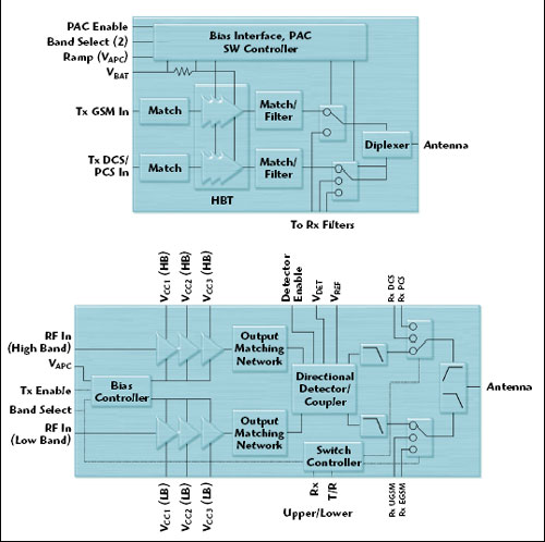
Fig. 3 PA front-end module
For linear PA applications (CDMA, WCDMA, etc.), there is no CMOS controller chip and, instead, the bias circuitry is included on the PA die. The bias circuit is typically a variation on the simple current mirror circuit.5 Over time, the bias circuits have become more complicated to satisfy customer demands for improved battery lifetime. Naturally, as the level of desired functionality increases, the design complexity of the bias circuit continues to increase accordingly.
As the PAM transitions to a front-end module (FEM) or a system in package (SiP), other features, such as couplers, detectors and matching components, may migrate to being on-chip (for GaAs PAs). One of the more difficult aspects of integrating a system on a chip is that the power amplifiers in a CDMA system are preceded in the RF chain by a filter and followed by a duplexer. These create a natural boundary to single-chip integration. However, on the module level, adding customer features while lowering the cost will continue to drive higher levels of integration.
Device Technologies
Many different technologies are used in a PA module. Here, the focus will be on the PA MMIC (power amplification chain) only. There are trade-offs associated with all of these technologies for use in power amplifiers. However, there are standards for many of the parameters such as gain, linearity and ruggedness, and one only needs to meet them (over bias, temperature, voltage). Other parameters, like power-added efficiency (PAE), cost and time to market, are key reasons for choosing a particular technology since they provide some benefit to the end user (and are not just pass/fail specifications).
Characteristics that distinguish good PA technologies include low cost (die-size, reproducibility and yield), good reliability and robustness, high power gain (device and assembly related), high breakdown voltage, good linearity and positive turn-on voltage. Key specifications for the finished PA include cost/size, ruggedness, gain, linearity (multiple channels) and efficiency.
For initial handset PAs, the device technologies of choice were LDMOS and Si bipolar, since these were readily available from their use in other power applications and the supply voltages (5 V) aided in keeping these technologies competitive. The Si bipolar designs consisted of discrete power devices integrated on module.2 GaAs MESFETs were later used, but lost market presence due to the negative gate voltage requiring a DC-DC converter (added cost), inferior size and yields compared to GaAs HBTs. In the late 1990s the supply voltage for PAs was lowered to a nominal of 3.4 V. This means that the PA needs to operate anywhere from 4.2 V (on charger) to 2.8 V (battery almost dead). LDMOS and Si BJT, possessing many of the important characteristics, began losing market share to GaAs HBTs based on PA performance metrics such as gain, linearity and power-added efficiency. Currently, GaAs HBTs dominate both the linear and saturated PA markets due to superior performance. Handset manufacturers favor GaAs HBT PAs due to their better efficiency, especially at higher frequencies. In addition, the simpler process (compared to silicon), excellent yield and high power density have all contributed to this market preference. A more detailed consideration of the competing technologies now follows.
D-mode MESFET and HEMTs provide good PAE and linearity, good RF integration capability and provide the best option for RF switching. However, the negative supply voltage (as mentioned earlier) and manufacturing issues do not make them competitive for PAs. E-mode MESFET/HEMTs do not require a negative supply, but provide limited output power for PAs, and have manufacturability worse than D-mode, Si, or bipolar technologies. Si (SiGe) bipolar requires a positive supply, has both excellent turn-on control and manufacturability, but has inferior quality passives, and non-competitive PAE and gain for many PA applications. Si PAs can be competitive at lower frequencies (cellular CDMA), but are not competitive at higher frequencies.6 RF CMOS/LDMOS does not require a negative supply, but the PAE is non-competitive at higher frequency bands,7 the lower power density leads to larger die and inferior on-chip passives limit integration capability. In addition, the long turnaround times and mask costs lead to expensive development costs. III-V HBTs do not require a negative supply, have excellent turn-on control (although higher than Si), competitive PAEs and high power density. The simple process enables fast turnaround times (time to market advantage) and minimizes mask costs. Also, a MESFET can be integrated into a III-V HBT process8 adding design flexibility while maintaining a simple manufacturing process.
There is currently a great deal of research on Si (BiCMOS and CMOS)-based technologies since they offer the promise of “system-on-a-chip.” These solutions will only be acceptable, however, once the development time and cost of the PA is made to coincide with the rest of the development of the system. This will also limit the flexibility of PAM fabrication since the optimum technology for a given function of the PAM cannot necessarily be used. Other emerging technologies (InP, GaN and SiC) will have to prove that they are capable of competing on cost, manufacturability and demonstrate significant performance improvements to displace the incumbents. As for which technology is “best” for PA applications, it is really more a question of how to use/partition all of the various technologies where they make sense, rather than selecting only one and compromising system performance.
Emerging Technologies and Topologies
The key performance drivers for power amplifiers are improvements in linearity and efficiency characteristics; these specifications have become progressively more stringent with each generation of system. One of the main focuses for PA design has been on reducing the battery consumption by improving efficiency.9 This is driven by matching the PA’s performance to the transmission probability curve, making the PA more efficient where it transmits most of the time. Typical techniques to achieve this include reducing average current consumption of the PA (bias current adjustment or re-configure the PA with switches), reducing average supply voltage to the PA (adjust voltage as a function of RF output level or using envelope following/tracking) and adjusting the load-line (electronic tuning of output match or dynamic load-line adjustment). Another method for improvement is to use pre-distortion or similar schemes to improve the linearity then trade it off for improved PAE.10 An example of a design that improves battery life is an AutoSmart™11 power amplifier technology that internally adjusts the RF transistor bias level throughout the dynamic operating range to minimize battery current consumption and ensure sufficient linear performance to meet CDMA system requirements. The result is a significant savings in average battery current without the complications of a system-supplied mode function signal or analog bias control. These new bias circuits represent a significant advance over standard bias techniques used in the past. Another observed trend in linear PA applications is the removal of the isolator from between the PA and the antenna.12,13 The removal not only means that the PA must survive potentially worse mismatch conditions, but it is being required to demonstrate consistent performance over a 4:1 VSWR circle rather than just at the 50 ? match point. This has resulted in the development of so-called load-insensitive power amplifiers (LIPA™) that have consistent performance over this 4:1 circle.
While there are many other topologies and techniques for power amplifier improvement (many flavors of Doherty, envelope tracking, integrated DC-DC converters) that have been published, there still will be a fairly long lead time until these start to become ubiquitous, if at all, in commercial products.
Transceivers
Integrating the RF Front-end System
A cellular phone based on the GSM standard and operating on a time-duplex basis lends itself to a switch-only implementation of the RF front-end system. The simplest GSM handset operates in a single-band mode and requires only a single-pole two-throw switch, a receiver filter and matching network, and a power amplifier. The current market demand for increased functionality, however, requires that GSM phones support up to four different bands. Consequently, a quad-band GSM phone may include up to four transmit paths and four receive paths. The transmit paths require at least two power amplifiers: one for the GSM850 and GSM900 bands and a second for the DCS-1800 and PCS-1900 bands. Add to this the individual filter and passives required for the receive path, and the result is a total of six paths, which increases the design complexity and component count. The challenge to provide increased functionality without increasing complexity or component cost is compounded when a second wireless system, such as 802.11b WLAN, is added on the same platform to form a multi-mode device. Since the GSM and 802.11b operate at different frequency bands, their respective front-end components cannot be shared, as both modes require their own set of power amplifiers, switch and diplexers, receiver-matching circuits, and filters on the PCB. For these RF front-end functions, the best approach is to use pre-integrated modules and packages. Power amplifier modules, in the form of multi-chip modules containing power amplifier and power control logic functions, already exist for multi-band cellular and multi-mode 802.11a/g WLAN applications. Similarly, RF front-end modules containing the switch and diplexer and the receive filters are also available. In the future, a combined cellular and WLAN RF front-end subsystem should also be available once the market opportunity justifies the investment in developing and commercializing such products.
Baseband Partitioning
Many of today’s cellular baseband chips are highly integrated CMOS system-on-a-chip (SoC)14 devices with either one chip containing both digital and analog functions, or separate chips for the analog and digital basebands. The choice between the two partitioning schemes is driven by many factors, including the future integration path.
The two-chip approach enables the most aggressive path for integration, as the analog baseband function is isolated from the “pure” digital circuits making up the digital baseband. Using this approach, the digital baseband can scale according to Moore’s Law to smaller and smaller CMOS geometries, something not easily accomplished with the analog circuits. Another benefit of this partitioning scheme is the possible integration with other digital CMOS platform components — application processor, image processor, memory, etc. — in a SoC. With the advent of digital RF interfaces, such as those currently being defined in the DigiRF standard body, the analog circuits may disappear entirely in the baseband. This approach calls for the definition of a standard high speed digital serial interface between the radio and the cellular baseband.
Similar efforts are being pursued by the WLAN vendors in their definition of a standard serial interface in the JEDEC61 body. Once the digital serial interfaces are standardized, the cellular baseband functions can be integrated more cost effectively, with either complementary digital functions or with other modes of wireless baseband circuits.
RF Transceiver Integration in CMOS
Although the RF front-end system may be combined using package or module technology and the baseband functions integrated with other digital functions on the platform, developing a highly integrated multi-band/multi-mode transceiver is an extremely challenging task. Recent advances in RF design make it possible to produce single-chip multi-band GSM/
GPRS transceivers in CMOS without compromising performance. However, delivering the cellular multi-mode RF/mixed-signal integrated circuits in CMOS is even more challenging, requiring innovative new circuit architectures and technology, as well as advanced design skills.
The key challenge is to integrate the RF transmitter and receiver circuits along with the frequency synthesizers, oscillators and filters while supporting multiple wireless modes and frequency bands. For example, the transceiver may be designed to support GSM, EDGE, WCDMA and high speed data packet access (HSDPA) modes, but will also be required to support frequency bands ranging from GSM at 850 MHz to over 2.1 GHz for UMTS, with various channel bandwidths. Furthermore, the multi-mode cellular transceiver must meet the stringent performance requirements — better than –102 dBm sensitivity and 4 dB margin on the transmit mask for GSM/GPRS. Designers therefore must be extremely careful to select the best silicon technology and transceiver architecture that will best optimize their design for cost and performance. For multi-mode integration, CMOS is the ideal process technology, as it enables the efficient implementation of digital signal processing (DSP) circuits with RF/mixed-signal circuits on a single chip. A CMOS transceiver leverages the lower cost and higher performance scaling of Moore’s Law to a greater degree than the BiCMOS or SiGe processes. CMOS transceivers can offer IC performance and functionality comparable to BiCMOS components, and they can also provide lower component cost, lower power consumption and better stability in manufacturing, comparable to other digital CMOS products. The many commercially available GSM/GPRS, WLAN or Bluetooth CMOS transceivers demonstrate the viability of CMOS technology for high volume wireless transceiver products.
Low IF or zero IF (ZIF) architectures are the most suitable transceiver architectures for integration because, in both cases, the receiver and transmitter chains are designed to eliminate the need for external SAW filters. This provides a high level of integration and reduces the bill of materials (BOM) of the platform. The need for on-chip multiple mixers and oscillators is also eliminated, as both architectures convert the incoming high frequency signals directly into low IF or ZIF baseband signals. In addition, multi-mode operations are facilitated, as these architectures allow on-chip programmable filter structures to accommodate the variable channel bandwidth.
Designing cellular transceivers based on low IF or ZIF architectures is not a trivial exercise due to 1/f noise issues associated with CMOS and the DC offset issues associated with ZIF.
Designers must be careful to:
• Minimize the effect of 1/f noise
• Design low noise RF front-end functions such as LNAs and mixers
• Reduce the phase noise of integrated oscillators
• Provide for high quality on-chip frequency synthesis.
One solution is to develop an entirely new architecture that has the ability to tolerate large amounts of digital noise. This architecture often involves advanced RF/mixed-signal circuit designs with a low intermediate frequency (low IF) and innovative DSP techniques that perform digital calibration and compensation of the analog non-idealities on chip.
Digital Baseband
Processor Capability and Trends
Adoption of features such as color display, cameras and converged capabilities would not be possible without advances in semiconductor technology, microprocessor architectures and embedded systems. It is for this reason, and to implement more advanced features such as 2D and 3D graphics, mobile multimedia, mobile IP and personal entertainment, that many of the emerging baseband processors have multiple processing cores.
The early generation analog cell phones consisted of a discrete single CISC-based microcontroller unit (MCU)15,16 core controlling a number of analog circuits. The move from analog to digital technology drove the need for a dedicated core processor to be added to the architecture. A block diagram of the current generation digital cellular baseband architecture is shown in Figure 4. This dual-core architecture, consisting of an MCU and DSP, evolved from several discrete parts to a single application-specific integrated circuit (ASIC) in the mid-1990s.

Fig. 4 Dual-core processor architecture.
The additional performance required to support packet data (that is, EDGE/GPRS) was addressed by increasing the clock speed for both cores, adding hardware accelerators for encryption/decryption and adopting support for burst mode flash memory. Dual-core cellular baseband ICs across the industry use approximately the same process partition, with the DSP performing signaling tasks and serving as a slave processor to the host MCU (a RISC core), which runs the upper layers of the communications software protocol stack. The Layer 1 signal processing tasks handled by the DSP include equalization, demodulation, channel coding/decoding, voice codec, echo and noise cancellation, and audio equalization (see Figure 5).
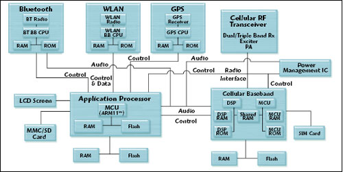
Fig. 5 Dual-core processor task partition.
The host MCU manages the radio hardware while performing the upper layers of the network protocol stack, subscriber identity, user interface, battery management and the non-volatile memory for storage for the phone book. The convergence of Internet and the introduction of wireless packet data service requires all the wireless processing capability of today’s cellular baseband architecture, together with the additional processing resources needed to support applications containing multimedia and graphics, inclusive of H.264 and MP3 engines.
The current dual-core baseband architecture was not designed to support the feature requirements of converged devices, and as a result, today’s smart phone architecture provides additional processing resources by adding a discrete application processor to the discrete dual-core cellular baseband IC, as shown in Figure 6. Each processor requires its own memory system comprised of RAM and flash. Support for additional wireless networking, such as Bluetooth and WLAN connectivity, requires additional modules for each function, including radio transceivers, digital basebands, RAM and flash components within the module. This approach yields a system architecture having a minimum of three, or as many as six, CPUs, each with its own dedicated memory system, peripherals, clock generator, reset circuit, interrupt controller, debug support and inter-processor communications software.
Fig. 6 A typical smart phone architecture.
Having separate, independent processing resources requires a sophisticated inter-processor communication bus to perform data exchange and control. The inter-processor communication bus becomes a formidable design challenge to software and hardware designers, as the need to exchange real-time audio, compressed video, high speed packet data and closed-loop system control becomes critical to achieving the desired product features and use cases. Supporting a full duplex digital audio stream between the cellular baseband and the 802.11 module, for example, while simultaneously supporting packet data communications between the application processor and cellular baseband, requires a sophisticated inter-networking approach, leading to reduced processing performance available for end-user applications and increasing power consumption. In the dual-core solution, the performance capability of the MCU is enhanced to serve user applications and cellular call processing roles. In this case, the performance of the MCU is shared between PDA applications and the rigid timing requirements associated with running the communication protocol stack. Consequently, this approach makes it difficult to meet end-user application environment with rich multimedia applications, besides exposing the wireless system to potential security and virus attacks through applications downloaded into the device.
The three-core approach, like the one proposed by Siemens and Motorola, merges dual-core cellular baseband architecture with a third (MCU) core dedicated to non-cellular user applications. This approach eliminates the performance conflict between the communication protocol tasks and multimedia workloads, and addresses the security issues that are prevalent in the dual-core partition. The complexity of inter-processor communication among the three cores is not reduced, because the application processor must interact with both the DSP and the call processor MCU. The current generation smart phone architecture uses a separate baseband modem for each wireless network type. The disadvantage of managing separate modems to support multiple wireless networks is three fold:
• Inter-processor communication
• System power and standby time
• Cost
The current generation smartphone software architectures, as shown in Figure 7, have evolved from feature-phone implementations that provide enhanced services in the modem software (on the MCU side). The inter-processor communication provides the bridge between the application environment on the application processor and the modem software on the baseband processor. This architecture, due to its evolution, includes complex interactions, redundancies and duplication between the application environment and the modem software. The mobile baseband processor will tend to have the following features to accommodate the wireless technology and application demands in the emerging handset market:

Fig. 7 Current smart phone processort architecture.
• Single-core baseband modem: Either a single high speed DSP core or an array of DSP cores17,18 like that used by Pico systems, Sandbridge or Morpho will form the Core baseband modem that performs all the complex signaling protocol in layers (L1, L2 and L3) for (WCDMA, UMTS) standards. The performance needed to support high speed wireless data is achieved by using a combination of embedded non-volatile memory (NVM) and RAM. The architecture incorporates an L1 cache to improve performance when using slower memory systems. It also provides additional power savings by reducing the frequency of accesses to the memory system.
• Dedicated application processor: A 9xx ARM core, on-chip L2 cache and a full complement of peripherals.
• System security: The architecture will include security framework, comprising both hardware and software elements required for a wide range of security services and applications.
• Small footprint: The multicore or multiprocessor architecture would use a single19 package — a package or multiple small packages whose area is less than 13 × 13 mm.
The evolution of technologies has significantly changed our daily life. In the future, this evolution will happen even faster. To make our technical world even more user friendly, the concept of a so-called ‘smart environments’ has been developed. In such intelligent environments, as many actions as possible are triggered and executed automatically, thus minimizing the number of manual activities of the user. Smart environments are evolving in the office field and in public life. Furthermore, they are slowly beginning to find their way into private homes and into automobiles. An illustrating scenario for a smart environment is the intelligent automobile (smart car) that automatically identifies its driver and his/her preferences. When the smart key in the pocket of a driver approaches, the doors will be unlocked, the pre-programmed settings for the driver seat and the rear-view mirrors will be adjusted, and the favorite parameters for the air conditioning will be recalled and executed. One could even remotely start the car and turn on the heater ahead of time. Although such features are available in certain luxury cars, it is done through front panel programming or through proximity RF transmission systems and consequently lacks the adaptability and convenience of a full wireless solution. This inspiring example indicates a dramatic change of the coming world of mobile communication. Unprecedented, wireless networks will evolve their limited set of services to an unlimited variety of applications, and today’s set of wireless terminal types will expand considerably. The introduction of UMTS (Universal Mobile Telecommunications System) will only be a very first step into this new wireless world.
Evolution of Digital Baseband Processing Requirement
For the ideal case of a digital realization of all components, the processing power has to be considered to develop a sensible strategy for a hardware/firmware split. Figure 8 shows the processing power of a GSM system. It can be seen that the RF functionality will need approximately 1000 GIPS (giga instructions per second) and IF functionality will need about 100 GIPS. For baseband, a processing power of 10 GIPS will be necessary.

Fig. 8 Processing speed requirements for 2G/3G phones.
If GSM is combined with EDGE (Enhanced Data Rates for GSM Evolution) to achieve higher data transmission rates (up to 384 Kbps),20 the processing power increases for RF to 2000 GIPS, for IF to 200 GIPS and for BB to 30 GIPS. This is a factor of between two and three more than for GSM. For UMTS with an average data transmission rate of 400 Kbps (max. 2 Mbps) the necessary processing power increases tenfold compared with GSM. That means 10000 GIPS for RF, 1000 GIPS for IF and 100 GIPS for BB. Additionally, depending on the complexity of applications, 0.001 to 1 GIPS must be reserved. Figure 8 clearly shows that the current processing capabilities cannot enable a software-defined radio architecture due to insufficient processing power. The typical processing power of ASICs with approximately 20 GIPS is far below the required 10000 GIPS for the RF component of UMTS.
Therefore, it is necessary that the next generation of mobile communication architecture consider the hardware/software partitioning. For the digital components, power consumption, chip size and programmable ICs are the criteria, and a question of whether to use ASICs, FPGAs (field programmable gate array), DSPs (digital signal processor), CISC (complex instruction set computing) or RISC (reduced instruction set computing) processors. ASICs are intended for a specific purpose and offer the highest integration densities and lowest power consumption, but they are not programmable and cannot be modified. FPGAs are standard components and are programmable once.21 Using such devices with low power consumption and small chip size allow a shorter time to market.
DSPs for signal processing and CISC /RISC processors for handheld application are freely programmable and, therefore, can be used with greater flexibility. Standardized hardware and standard processors allow the development of hardware independent software, which is transferable to different mobile terminals. However, their power consumption is higher and their chip sizes are larger than those of ASICs and FPGAs.
Hardware/Software Split
The growth of the mobile phone market is being driven by consumer demand for more functionality in smaller and more affordable handsets and handhelds for high speed wireless data services and multiple wireless technologies (multi-mode). While high speed data service is made possible by advances in 2.5G networks (GPRS, CDMA 1¥RTT) and 3G networks (UMTS/WCDMA, cdma2000), the reduced size and cost of the handsets and handhelds are enabled by the scaling of silicon technologies and the integration of key component building blocks, such as the RF transceiver. Two examples exemplify the popular approaches currently adopted for baseband partitioning.22
Most of today’s multi-mode platforms are built with the combination of independent wireless subsystems on the same platform, as shown in Figure 9. For example, a multi-mode phone supporting GSM, W-CDMA, Bluetooth and GPS may be constructed with a GSM/WCDMA baseband, an applications processor, power management IC, memory IC, a GSM RF transceiver, discrete components making up the W-CDMA transceiver, a single-chip Bluetooth system, a two-chip GPS subsystem, and a multitude of RF front-end and passive components to support the various wireless capabilities. In the described phone example, the single-chip Bluetooth and the two-chip GPS chipset are connected to the application processor, while their respective software drivers are embedded into the operating system that controls the operation of the entire platform. Also, since these are independent “stand-alone” systems, the Bluetooth and the GPS subsystems may operate concurrently during a network call established by the handset. While the system-level integration of various wireless capabilities makes sense for some applications, it doesn’t result in a solution that is optimized for the lowest cost or the smallest form-factor handsets
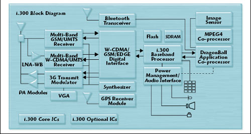
Fig. 9 Typical GSM/WCDMA multimedia handset.
The comparison shown in Figure 10 clearly demonstrates that today’s digital circuits provide the required processing power of 10 MIPS for the BB of UMTS. Therefore, the signal processing of RF, IF and parts of BB still have to be realized by analog hardware. To decide which parts of the baseband circuitry will form the digital front end, the processing power of the WCDMA-downlink-receiver (wideband code division multiple access) shown in Figure 9 is investigated in detail.
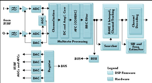
Fig. 10 Typical WCDMA system functional blocks.
The low pass-filtered and digitized signal is fed into to a digital filter for data pre-treatment. Compensation for multi-path fading and run time delays are performed at the RAKE receiver and the searcher loop. Hereafter the signal is de-spreaded in the channel decoder. Table 1 shows the correlation between the components of the WCDMA receiver and the required processing power. Digital filter, searcher, RAKE receiver, MRC (maximal ratio combining) and turbo-decoder require much more processing power than 10 MIPS and have to be realized by analog hardware23 (ASICs, or FPGAs). However, channel estimator, AGC (automatic gain control), AFC (automatic frequency control) and de-interleaving call for a DSP-based firmware realization because here the required processing power ranges from 10 MIPS to 14 MIPS.

Predictably, the evolution of semiconductor technology will shift the hardware/firmware split, with increasing processing power of future digital processors. The portion of software or firmware-based components is growing continuously and will replace hardware-oriented microelectronic architectures step by step.
Trends in Digital Semiconductor Technology and Roadmap
The decreasing feature size relates to the increasing integration density and the usage clock frequencies shown in Figure 11. The processor speed nearly doubles every three years and the integration density also increases exponentially. The extrapolation of the data allows an estimation of semiconductor technology evolution in the future. Conservatively, the large-scale availability of a cognitive radio can be expected no later than 2020. However, targeted applications for cellular/PCS/WiMax base stations will start emerging by 2006. Currently, semiconductor technology for the mobile communication of the third generation cannot exist without analog hardware components due to nonavailability of a power efficient multicore processor and also the cost of the solution.

Fig. 11 Feature size (a) versus clock speed (b).
From Table 1, it can be seen that, with increasing processing power, the “maximal ratio combining” with 24 MIPS will be replaced by a software-defined solution first. The turbo decoder with 52 MIPS will follow next. The software version of the RAKE receiver with 650 MIPS represents a larger step and will follow after a longer time period, but will also be available for 4G in time.24 Extrapolated data shows the possible hardware/software split of future handset terminals.
Typically, in a transceiver, the most power consuming part is the analog front end. Due to the physical size of the analog components, a relative large chip area is necessary. Furthermore, some steady trends can be observed following the path of the signal from the antenna towards the low frequency side — going along with the signal, the necessary sample rates are decreasing while the complexity of algorithms is increasing concurrently. For an additional clarification, these facts are sketched in Figure 12.
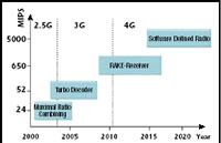
Fig. 12 Roadmap for hardware/software split.
An important concept that emerges from these trends is that there is a clear migration path towards higher integrated radios through minimizing the analog components in the design. Transitioning into a more digital architecture allows easier migration towards a cognitive radio.
All three objectives, the overall power consumption, the integration density and the necessary chip area, can be optimized by strictly following this paradigm. However, parasitic effects may degrade the simplified analog front end to an extent that the system performance becomes seriously degraded. These effects will have to be either compensated by a proper determination of the silicon process or through algorithmic means and rely as much as possible on digital circuits. By this, the hardware designer will benefit from the fast evolution of digital microelectronics technology. A corrective feedback signal from the digital circuit back to the analog front end should be considered as a compromise, if a suitable algorithm is not available.
To bring about a convergence of baseband and RF hardware integration to a single die, leading to multi-mode and multi-standard cellular handsets, the current hardware software interface has to be flexible enough to accommodate the rapid advances in silicon technology. The obvious benefits are lower cost BOM and performance. A paradigm change of the hardware design philosophy will accelerate the appearance of mobile cognitive radio multimedia terminals.25
Conclusion
The number of semiconductor technologies being applied in the RF and microwave marketplace has grown significantly over the past 20 years. In applications and frequency ranges where GaAs had been required to meet performance requirements, Si CMOS and BiCMOS technologies have taken over. This trend will continue into the future as existing Si technology generations transform into higher performance successors that push their usefulness to even greater frequencies. Application spaces that were once thought too high in frequency for Si-based processes will, in fact, become dominated by silicon.
In a similar fashion, the trend away from pure analog radio implementations will be fueled by digitally rich architectures as processing speeds increase and the power per MIPS continues to decrease. Multi-mode radios will also move away from hardware specific implementations to software definable and re-configurable architectures.
References
1. W. Andrews, “CMOS: The Technological Dark Horse is Off and Running in ’84,” Electronic Engineering Times, February 13, 1984, C7-C10.
2. R. Jos, “Future Developments and Technology Options in Cellular Phone Power Amplifiers: From Power Amplifier to Integrated RF Front-end Module,” 2000 Bipolar Circuits and Technology Conference Digest 2000, pp. 118–125.
3. V. Ramachandran, A.J. Joseph, J.B. Johnson, M.D. Gallagher, P.O. Brandt, L. Tilly, D.R. Greenberg, W.E. Ansley, U. Gogineni, D.L. Harame and J.S. Dunn, “A Fully-manufacturable 0.5 mm SiGe BiCMOS Technology for Wireless Power Amplifier Applications,” GAAS 2002, 23–27 September 2002, Milan, Italy, pp. 303–306.
4. T. Shimizu, “Improved Si-LDMOS Process Enables 65% Reduction in Mounting Area and Incorporation of Automatic Output Power Control Function,” Renesas Edge 2004, Vol. 5, p. 13.
5. P. Walters, P. Lau, K. Buehring, J. Penney, C. Farley, P. McDade and K. Weller, “A Low Cost Linear AlGaAs/GaAs HBT MMIC Power Amplifier with Active Bias Sensing for PCS Applications,” Digest of the 1995 GaAs IC Symposium, pp. 67–70.
6. K. Nellis and P. Zampardi, “A Comparison of Bipolar Technologies for Linear Handset Power Amplifier Applications,” IEEE Journal of Solid-State Circuits, Vol. 39, No. 10, Oct. 2004, pp. 1746–1754.
7. C. Weitzel, “RF Power Amplifiers for Cellphones,” 2003 GaAs Mantech Conference Digest, Paper 2.2.
8. US Patent 5,250,826.
9. T. Fowler, K. Burger, N.S. Cheng, A. Samelis, E. Enobakhare and S. Rohlfing, “Efficiency Improvement Techniques at Low Power Levels for Linear CDMA and WCDMA Power Amplifiers,” 2002 Radio Frequency Integrated Circuits (RFIC) Symposium, June 2–4, pp. 41–44.
10. J. Staudinger, “An Overview of Efficiency Enhancements with Application to Linear Handset Power Amplifiers,” 2002 Radio Frequency Integrated Circuits (RFIC) Symposium, June 2–4, pp. 45–48.
11. SKY77163 Product Data Sheet.
12. SKY77104 Product Data Sheet.
13. A. van Bezooijen, C. Chanlo and A.H.M. van Roermund, “Adaptively Preserving Power Amplifier Linearity Under Antenna Mismatch,” 2004 IEEE MTT-S International Microwave Symposium Digest, Vol. 3, June 6–11, 2004, pp. 1515–1518.
14. International Technology Roadmap for Semiconductors, chapter entitled “System-on-a-Chip,” http://public.itrs.net/, 1999.
15. S. Rusu and G. Singer, “The First IA-64 Microprocessor,” IEEE Journal of Solid-State Circuits, Vol. 35, No. 11, 2000,
pp. 1539–1544.
16. K. Dieffendorff, “Power 4 Focuses on Memory Bandwidth,” Microprocessor Report, Vol. 13, No. 13, 1999.
17. J. Lin, “Chip-package Co-design for High Frequency Circuits and Systems,” IEEE Micro, Vol. 18, No. 4, 1998, pp. 24–32.
18. A. Cataldo, “Facing Size, Cost Issues, Intel Pared Penthouse Pentium 4,” EE Times, Dec. 18, 2000, p. 26.
19. E. Davidson, “Large Chip vs. MCM for a High Performance System,” IEEE Micro, Vol. 18, No. 4, 1998, pp. 33–41.
20. E. Davidson, et al., “Long Lossy Lines (L3) and Their Impact Upon Large Chip Performance,” IEEE Trans-CPMT-B, Vol. 20, No. 4, 1997, pp. 361–375.
21. R. Shukla, et al., “Flip Chip CPU Package Technology at Intel: a Technology and Manufacturing Overview,” Proceeds of the 49th Electronic Components and Technology Conference, May 1999, pp. 945–949.
22. L. Schaper and T. Lenihan, “Passives Go into Hiding,” Advanced Packaging Magazine, Feb. 1998, pp. 22–26.
23. C. Panasik, “Overcoming Obstacles to 3G Wireless Technology,” Communications Systems Design, January 2001, pp. 11–12.
24. J.H. Reed, Software Radio – A Modern Approach to Radio Engineering, Prentice Hall, 2002.
25. E. Buracchini, “The Software Radio Concept,” IEEE Communications Magazine, Vol. 38, No. 9, Sept. 2000, pp. 138–143.
Peter M. Bacon received his BSEE and MSEE degrees from Lehigh University in 1983 and 1985, respectively, and his MBA degree from Boston University in 1994. In 2003 he joined Skyworks Solutions Inc. He is currently senior engineering director of the linear products business unit overseeing GaAs- and Si-based product development activities for a variety of market applications.
Chandra Mohan received his BS degree in electrical engineering from the National Institute of Technology, Calicut, India, and his masters degree in electrical engineering from the Indian Institute of Technology, New Delhi, India. He is currently responsible for developing silicon solutions for high performance wireless infrastructure applications at Skyworks Solutions Inc., Irvine, CA.
David J. Fryklund received his ASEE degree from Wentworth Institute in 1969 and his BS degree in electrical engineering technology from the University of Massachusetts in 1972. He worked a total of 21 years at M/A-COM, and was responsible for developing the GaAs switch product line. He is presently employed at Skyworks Solutions Inc., where he has spent a total of 12 years in various managerial positions.
P.J. Zampardi received his BE degree in engineering physics from the Stevens Institute of Technology in 1986, his MS degree in applied physics from Caltech in 1988 and his PhD degree from the University of California at Los Angeles in 1997. Since 2001 he has been at Conexant/Skyworks Solutions, where he manages the Device Design and Technology Characterization Group. He has authored or co-authored over 100 papers related to circuits and devices, and actively participates in the BCTM and IMS technical committees.