
Ever since Bell Lab physicists Shockley, Bardeen and Brattain invented the transistor, this little solid state device has been constantly evolving; leveraging the advantages of different semiconductor and process technologies and addressing an increasing number of applications once reserved for tubes. Sixty-plus years later — driven by a number of promising commercial and defense-related markets — transistors (and MMICs) specifically targeting high power applications in the RF and microwave frequency range continue to be the focus of sizable research and development.
Among the changing landscape of RF/microwave semiconductor developments, devices with material properties that can sustain high electric breakdown are of particular interest. To understand the state of the high power transistor market, we spoke to a number of leading vendors. Our discussion was mostly concerned with devices that could produce in excess of 30 W at UHF/VHF frequencies and above (up to X-band). These are the high-power transistors required for avionics, radar, EW and wireless infrastructure applications. Although these devices are also found in medical equipment, those applications will not be part of our focus in this article. The following is a summary of our correspondence.
High Power Transistor Technologies and Applications
Within the last six months alone, the Journal has published over a dozen papers on Laterally Diffused MOS (LDMOS), Gallium Nitride (GaN), Silicon Carbide (SiC) and High-Voltage Vertical FETs (HVVFET). The principle market segments for high-power, high-frequency transistors are wireless infrastructure (3G, 3G+, WiMAX/LTE base stations and backhaul), defense and military applications (radar, jamming, counter-measures, guided weapons, etc.) and broadcast and communication satellites (SatCom). The factors that will decide whether a technology dominates a given application include performance (linearity, efficiency), reliability (ruggedness and thermal considerations), size, cost and legacy.

Figure 1 An overview of preferred transistor technologies for 2008 design-ins as a function of power and frequency (courtesy of NXP Semiconductors).
Figure 1 maps the various high-power semiconductor technologies relative to their operating frequencies and available output power. With an understanding of the power and frequency requirements for a given application, this graph provides a rough guide to the leading technologies today. Implicit in this representation are regions where one technology overlaps another due to its cost advantage. This cost can be related to higher production costs (complexity, less mature processes or lower volume production all drive up costs) as well as replacement costs (a technology missed the critical time-to-market). As process technology advances and new standards (i.e. 4G) provide new opportunities to enter a market, technology dominance in any particular region is subject to change. These factors will be discussed later in this article.
Radar and Avionics
According to ABI Research, the demand for the pulsed RF power devices (greater than 5 W of peak output power and frequencies up to 3.8 GHz) is expected to show solid growth over the next five years, in part due to a worldwide upgrade of air traffic control systems including new avionics transponders and air navigation systems.1 In response, many semiconductor manufacturers are attempting to enter the avionics, L-band, S-band and sub-1 GHz radar markets. Competitive technologies such as GaN and SiC devices will be vying for market share along with the more established silicon-based technologies. With the entry of many would-be players, competition will be fierce. Companies that have an established track record working with government agencies and defense contractors will naturally have an advantage over new entrants.
Long-range radar systems operating from VHF thru S-band are demanding increased performance from the RF power amplifier in order to support the required improvements in system ranging and sensitivity. A key lesson learned from the crisis on 9/11 was the need to extend the pulse width to at least 300 µs for long-range radar as well as the ability to increase the operating dynamic range of the power amplifier.2
UHF/VHF Radar
Historically, silicon Class C amplifiers were limited by heat dissipation due to the potential for thermal runaway during long pulses (> 300 µs) and high peak powers. Military applications were among the first to use wide band gap (WBG) devices, especially with the SiC MESFETs being developed through broadly financed DARPA and DoD programs in the US.3 Recently, Microsemi's Microwave RF Power Division developed its WBG SiC technology in support of the new longer pulse radar systems and avionics being developed from VHF thru S-band.
The state of material technology has progressed to the point where Microsemi can build high power devices with reasonable yields and consistent performance. In 2008, the company introduced its first two RF power transistors utilizing silicon carbide technology for high power VHF and UHF band pulsed radar applications. The two Common Gate N-Channel, Class AB, SiC Static Induction Transistors (SIT) are capable of providing 1000 W, pulsed (300 µsec pulse width, 10 percent duty cycle) from 406 to 450 MHz and 1250 W pulsed at 150 to 160 MHz.
In January, the company made good on its promise to extend SiC technology to higher frequencies by introducing a new family of power transistors and modules designed for S-band (3.1 to 3.4 GHz) pulsed radar. The new products include a 65 and 100 W power transistor and two Power Solution Modules TM rated at 180 and 200 W (100 µsec pulse width and 10 percent duty cycle). The modules demonstrate 40 percent collector efficiency and power flatness of less than 0.5 dB, utilizing the company's advanced chip design and processing enhancements for high power and high gain.
Around the same timeframe (December 2008), HVVi Semiconductors announced its first product to target the UHF-band weather and long-range radar markets using its High Voltage Vertical Field Effect Transistor (HVVFET™) architecture. The company's 50 V device offered 175 W pulsed, 55 percent drain efficiency, 25 dB of gain for a pulse width of 300 µsec and pulse duty cycle of 10 percent at VDD = 50 V and IDQ = 50 mA. The UHF part also provided a boost to system reliability by withstanding an output load mismatch corresponding to a 20:1 VSWR across all phase angles at rated output power and operating voltage across the entire frequency band.
L-Band Radar
This new device, based on the company's HVVFET, followed the earlier releases (October 2008 at European Microwave Week) of three devices with pulsed output powers of 60, 100 and 250 W operating in the 1025 to 1150 MHz frequency band. These devices targeted airborne Distance Measuring Equipment (DME) applications, a transponder-based radio navigation technology that measures distance by timing the propagation delay of radio signals. The company also targeted ground-based DME (960 to 1215 MHz) with a 50 V device that provides 150 W, 20 dB gain and 43 percent drain efficiency.
These products expanded the company's portfolio across three L-band, pulsed radar applications: 1025 to 1150 MHz, 1030 to 1090 MHz and 1.2 to 1.4 GHz. The 1030 to 1090 MHz frequency band is used for IFF, TCAS and mode-S applications. For this market, HVVi introduced a pulsed (50 µs pulse width, 5 percent duty cyle) 35 W device (20 dB gain, 52 percent drain efficiency) and 300 W device (18 dB gain , 48 percent drain efficiency).
Meanwhile, Silicon Bipolar devices continue to be introduced into the market. Companies such as ST Microelectronics, NEC, Motorola and NXP have large Si-BJT product portfolios (to name a few). Last summer, M/A-COM announced a line-up of new high-power bipolar transistors designed for pulsed avionics applications such as ATC, DME and IFF systems, ranging from 960 to 1215 MHz. The Class C, Si-BJT pulse power transistors provide peak powers of 50, 350 and 500 W with gains of approximately 9 dB and 40 to 45 percent collector efficiencies. Integra Technologies also has an extensive portfolio of Si-BJT high power transistors targeting VHF through S-band pulsed radar applications, but they are also offering LDMOS devices as this technology continues to challenge the supremacy of the Si-BJT in the avionics and radar markets.
At last year's IMS in Atlanta, Freescale Semiconductor introduced the world's first 50 V LDMOS device for L-band radar with a demonstration of a class AB, long-pulse (300 µsec, 12 percent duty cycle) amplifier with peak power of 330 W, 17 dB gain and 60 percent drain efficiency operating between 1200 to 1400 MHz, a band used for ground-based, long-range surveillance radar applications. Freescale pointed to advantages, such as a standard voltage supply, low cooling costs and high reliability of pallet design and expected to demonstrate gain, efficiency and thermal resistance characteristics that would outperform other similar products in the market.
A year later at IMS in Boston, HVVi introduced its 500 W (19 dB gain, 50 percent drain efficiency) device operating with a 50 µsec pulse width, and 5 percent duty cycle adding to its portfolio of products with pulsed output powers of 25, 75 and 120 W (200 µsec pulse width, 10 percent duty cycle). The 500 W power level was also achieved by NXP Semiconductors this past November with an LDMOS device demonstrating greater than 50 percent drain efficiency and 17 dB of gain operating at 100 µsec pulse width and a 25 percent duty cycle at 1.4 GHz.
Japanese manufacturer Eudyna hit the 500 W mark and then some with an AlGaN/GaN HEMT 1.5 GHz power amplifier reported back in 2006 at the MTT-S IMS that year and an 800 W S-band transistor with linear gain of 14.0 dB, 56.4 percent drain efficiency covering a wide frequency range of 2.9 to 3.3 GHz (operating at 65 V, pulse width of 200 µsec and 10 percent duty cycle) reported just one year later at CS MANTECH. While Eudyna holds a strong position in the market, the company is at a disadvantage to domestic suppliers when it comes to US military opportunities due to (offshore) sourcing concerns. Not surprisingly, Eudyna markets its GaN HEMTs primarily to the WiMAX and LTE infrastructure markets where the majority of GaN manufacturers also have made considerable in-roads.
S-Band Radar
Integra Technologies addresses the S-band radar market with a comprehensive family of Si-bipolar devices (drivers, medium and high power amplifiers) operating from 2.2 up to 3.5 GHz (in bandwidths ranging from 200 to 400 MHz). The high power amplifiers have peak output powers up to 125 W (3.1 to 3.4 GHz) at 300 µs pulse width (PW), 10 percent DC and 140 W (3.1 to 3.5 GHz) at the shorter 100 µsec PW, 10 percent duty cycle. The company offers a LDMOS device operating at the same frequency and pulse conditions, which yields an output power of 154 W (29 W more) and an extra dB of gain (10.4 dB) at a lower drain voltage (32 vs. 36 V). This improvement in performance underlines the competition between technologies, even within the same company.
One domestic manufacturer going after the S-band radar market with GaN technology is RFMD. At last year's MTT-S IMS in Atlanta, the company debuted a 400 W pulsed output power GaN HEMT amplifier operating over the 2.9 to 3.5 GHz band (17 percent bandwidth). Under pulsed RF drive, with 10 percent duty cycle and 100 µsec pulse width, the amplifier delivers an output power in the range of 401 to 446 W over the band, with a drain efficiency of 48 to 55 percent when biased at a drain voltage of 65 V.
The wideband nature of GaN-based amplifiers, with the ability to easily cover 500 MHz to 3 GHz, make them well-suited for use in frequency agile pulsed applications such as military radar, air traffic control radar and communications jamming. In speaking with the Journal, RFMD remarked on GaN's higher efficiency for pulsed, CW saturated and linear applications, which improves thermal requirements and energy usage; showing 5 to 10 percent improvement over LDMOS and Si-Bipolar.
Ray Crampton of Nitronex further added that, "Radar applications require pulsed power in the hundreds of watts up to very high frequencies. This fits well because GaN devices offer improved robustness, higher efficiency, higher power density, higher gain and faster switching speed than competing technologies for today's broadband radar systems. GaN also offers the ability to replace TWTs with more reliable and robust devices." An example of Nitronex recent product offerings is the NPT1007, released last February. This is a 200 W device (based on two 100 W transistors) that targets military communication applications below 1.5 GHz and has notable "design-ins" in the 30 to 512 MHz band as well as bands up to 1 GHz, according to Crampton.
Meanwhile, TriQuint Semiconductor began investigating GaN technology back in 1999, and through subsequent years developed a baseline process that led to a DARPA contract focusing on technology maturity and wideband performance in 2005. This research and development effort resulted in a production-released 0.25 micron gate process supporting products from DC to 18 GHz and achieving power levels in excess of 100 W.
Commercial Markets – Wireless Infrastructure
Until four years ago, LDMOS covered about 90 percent of the high power PA applications above 2 GHz; the remaining market share belonged mostly to GaAs PHEMT technology.
WBG devices made a significant commercial breakthrough in 2006 when Eudyna and NTT jointly announced the first 3G network "test" deployment using GaN HEMT in Tokyo. New commercial offerings from Cree, RFMD and Nitronex soon followed, targeting both base station (3G, WiMAX) and general purpose applications. According to a 2008 GaN RF market report by Yole DŽveloppement, "GaN is currently positioned to challenge silicon dominance in the high power RF amplifier market estimated to be about $900 M in 2008."3 ABI Research has the RF power market somewhat below this figure at a predicted $800 M in 2011.1 But this challenge is not across the board, as LDMOS maintains an upper hand with pricing and legacy in certain sectors.
In the power market below 4 GHz, RF LDMOS transistors captured almost 70 percent of the total market in 2006. However, that number is predicted to go to 50 percent share of the RF power market in 2011, the ABI report forecasts. GaN may dominate most of the high-power markets at frequencies above 4 GHz, beyond the performance range of Si LDMOS. Eudyna Devices and Toshiba have wisely targeted the microwave (> 4 GHz) markets for much of their participation with GaN.
4G Opportunities
Market analysts point to product announcements by GaN manufacturers as indicators of their increased focus on WiMAX/LTE markets and a shift away from existing 3G/3G+ infrastructure, where LDMOS is the entrenched technology. Unfortunately, the WiMAX market in 2009 has been hit rather hard by the economic downturn. Building-out brand new networks from scratch, as is the case with WiMAX, requires hundreds of millions of dollars of capital. The current credit crunch along with a decrease in demand for broadband due to weakened consumer spending has led to many network build-outs being put on hold or delayed into next year.
Total sales of fixed and mobile WiMAX equipment fell 21 percent to US$245 M in the third quarter of 2008, from the second quarter's figure, and are expected to slide further in 2009 (a report in early May 2009 shows component makers revenue down 20 to 30 percent versus the year-ago quarter). Prior to the current slowdown, the GaN RF Market 2008 from Yole Développement had forecasted that the market size for GaN RF transistors could reach a level of about $100 M by 2010, largely due to strong penetration of WiMAX/LTE systems, as shown in Figure 2.
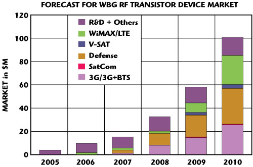
Figure 2 Projected RF markets for WBG transistors indicates most significant growth coming from 4G (courtesy of Yole Développement).
Still LTE rollouts are expected to be coming in the 2010 to 2011 timeframe and any WiMAX delays will shorten its current time to market advantage over LTE. Therefore, WiMAX deployment cannot afford to be postponed for too long. According to ABI Research, the LTE standard is being driven by operators, which is the key differentiator between it and preceding wireless technologies. CDMA and Asian operators who are early adopters will be the first to launch LTE. Existing UMTS operators will probably delay launch to extend the life of their existing HSPA networks and simplify the upgrade to LTE by slowly evolving their current architectures.
When network operators introduced HSPA, packet data traffic quickly exceeded voice traffic. In some cases, a four fold increase in data traffic occurred in just three months. Future WiMAX and LTE build-outs will be needed in order to serve 1.8 billion broadband subscriptions by 2012, according to a five year projection made by Ericsson in 2007.4 To get there, high power transistors will need to deliver on performance, size, reliability and price.
Technology
WiMAX faces strong competition from existing wireless services, making it essential that WiMAX infrastructure equipment be as cost-effective as possible. A rough rule of thumb is that for high volume cellular base station applications, LDMOS prices are on the order of $0.30 per W, GaAs is about $0.9/W and GaN is about $1/W. Performance-wise, linearity and efficiency for both WiMAX and LTE are also critical.
The importance of linearity and efficiency
Both WiMAX and LTE use OFDM as the core modulation technology in the downlink direction and thus have roughly similar performance for any given RF bandwidth and set of conditions. However, the uplink modulation techniques are somewhat different. While WiMAX uses OFDMA for the uplink, LTE uses single carrier frequency division multiple access (SC-FDMA), which has a significantly reduced Peak to Average Power Ratio (PAPR). WiMAX's OFDMA has a peak-average ratio of about 10 dB, while LTE's SC-FDMA's peak-average ratio is about 5 dB.
The higher PAPR associated with WiMAX and OFDMA requires that the amplifier handle the occasional high power levels that can greatly exceed the average signal strength without introducing unacceptable levels of distortion. One way to do this is to use a larger transistor operating far below its compression point, otherwise known as backing-off the amplifier. Unfortunately, amplifier efficiency takes a hit when the device is backed-off. At 2 GHz, the latest LDMOS has about 18 dB gain and is 65 percent efficient at the P1dB compression point. At a 6 dB back off point, the devices are typically -45 dBc WCDMA ACPR and 30 percent efficient. GaN offers slightly higher efficiency at 6 dB OBO.
Saving some green
According to Steven Theeuwen of NXP Semiconductors, "All the developments particularly for base stations and broadcast applications are driven by an ever increasing demand for higher efficiency, generally speaking. In turn this means less lost power, which means "greener" amplifiers. Higher efficiency does not only mean better use of RF power, but also reduces the energy necessary to remove the dissipated energy (cooling systems). Hence, improved efficiency helps twice, on amplifier and system level, to reduce overall power consumption. NXP claims leadership in delivering high efficient transistors and high efficiency concepts: developing the world's first fully integrated Doherty amplifier and the highest efficiency, discrete Doherty setup to date." (Ed. note: Based on LDMOS technology.)
At Mobile World Congress (Barcelona, Spain) in February, Freescale introduced its next generation (HV8) of LDMOS high power transistors, specifically targeting the stringent demands of high-data rates called for by WCDMA, WiMAX, LTE and Multicarrier GSM. The company claims that a primary benefit of the HV8 technology is the increase in operating efficiency, reducing the total power consumption of a base station system. This growing concern in "green" technology is driven by a global desire to cut energy costs and reduce the industry's carbon footprint along with the telecom provider's interest in lowering operating expenses.
The new devices introduced in February operate over the 860 to 960 MHz range, providing a power output range of 100 to 300 W and can be used in Class AB or C configurations. A symmetrical Doherty reference design using two transistors designed for multicarrier GSM applications was shown to deliver 58.0 dBm (630 W) peak power, 16.3 dB gain and a drain efficiency of 42.5 percent at an average output power level of 49.4 dBm (87 W) with good broadband linearity. Digital pre-distortion (DPD) evaluations showed the reference design to correct very well with six GSM carriers in signal bandwidths of up to 20 MHz.
According to Leonard Pelletier of Freescale, one of the most substantial system-related issues to consider when working with LDMOS is creating higher linearity through digital pre-distortion or feed forward error correction systems. With improvements in the correction capability of the architectures, the RF devices can be operated closer to their P1dB compression point, where the DC to RF conversion efficiencies are at their highest level. Improved linearity translates to improved efficiency and lower overall system costs.
Linearity and efficiency are also addressed with similar circuit architectures designed using GaN devices. According to Dave Aichele of RFMD, "The high terminal impedances of high voltage GaN devices make the amplifiers suitable for higher bandwidth Class AB amplifiers as well as applications that attempt to improve efficiency such as Doherty, linearity such as push-pull, and extreme bandwidth such as distributed techniques. Thanks to the high impedances (and low parasitics) of GaN HEMTs, these higher bandwidth amplifiers can utilize most any standard circuit architecture with enhanced simultaneous bandwidth/efficiency/power performance."
Ray Pengelly from Cree noted that, "There has also been much success designing very high efficiency Class E, F, inverse F, J, etc. PAs (with GaN). Doherty (Class A/B/C) with DPD have addressed a range of telecommunications applications. We today achieve efficiencies > 50 percent at peak power levels as high as 500 W. PAs associated with Envelope Tracking (ET), where the high breakdown aspects of GaN, allow drain voltage operation anywhere from 20 to 65 V again with efficiencies exceeding 50 percent. ET is particularly promising for multi-band telecom applications."
TriQuint recently introduced its PowerBand™ family of wideband, high power discrete transistors employing a "revolutionary" (and somewhat secretive) circuit architecture and process technology. The product portfolio is based on different semiconductor technologies, including TriQuint's GaAs PHEMT, LDMOS and GaN materials and processes. The first released LDMOS device operates from 500 MHz to 2 GHz and produces 30 W, P1dB (instantaneous bandwidth), while a GaN-based product that will produce 100 W P1dB CW is expected this year.
Changes to infrastructure architecture will have an impact on how devices will compete. There is a desire by network operators to move the power amplifier from the base of the radio tower closer to the antenna, so that the losses attributed to long cable runs can be eliminated. This will reduce the power required out of the amplifier. The Remote Radio Head (RRH) architecture can increase overall efficiency of the network from 13 to 15 percent up to 30 percent, but requires smaller and lighter amplifiers than those found in the cabinet of a base station. In addition, since the amplifier is on top of a tower, reliability takes on a new importance. The higher operating temperature, higher power density (and therefore smaller device periphery) and better efficiency are strong drivers for using GaN or SiC in the growing RRH market.
Scorecard
LDMOS
Summary: LDMOS was developed between the late 1980s and early 1990s and became the technology of choice for cellular and 3G base station applications, completely replacing the BJT with its higher gain and efficiency, and superior linearity. A typical 28 V LDMOS FET has a power density in the range of 0.7 to 1 W/mm with improvements occurring for each new generation.
Cree has reported GaN-on-SiC power densities of approximately 4 W/mm, meaning that less die size is required for GaN for the same amount of output power compared to LDMOS. Higher power density helps offset GaN's higher cost by increasing the number of die per wafer, yet not enough to surpass the price advantage held by LDMOS. Despite more chips per wafer, GaN is processed on smaller (SiC) wafer substrates whereas LDMOS is processed on much larger and cheaper Si wafers.
Benefits: Costs — LDMOS has the lowest cost per watt ($/W) ratio of any of the high power RF amplifier technologies. LDMOS also has some of the best Class AB linearity, gain, reliability and thermal resistance of any popular RF power technologies.
Where to use: LDMOS excels in high volume, medium to high power, linear systems with very stringent cost goals and very high reliability requirements.
Working with the technology: After years in the field, LDMOS has a solid track record. There are very highly developed and extensively used MMICs in the market place as multi-stage RF drivers and gain blocks. Freescale, for example, has a very extensive internal library of on-chip silicon passive components to design a wide variety of internally matched, temperature compensated, multi-stage RF MMIC devices with power levels ranging from 10 to 100 W. Large signal model (MET) includes thermal behavior.
Downside: LDMOS performance is excellent up to 3.8 GHz, but degrades rapidly beyond 4 GHz.
The Power Brokers: Freescale Semiconductor, RFMD, TriQuint, NXP Semiconductors, Integra Technologies, Infineon Technologies and ST Microelectronics.
GaN
Summary: GaNs early development dates back to the late 1990s, with funding largely from defense agencies such as DARPA. By the second half of this decade, GaN began to enter commercial markets with performance that challenged the prevailing technologies. Adoption of GaN has hinged on performance, cost and reliability, all of which has been favorable enough for the technology to make impressive penetration into several key high power markets.
Thermal management is key to achieving acceptable reliability. Because of this, GaN manufacturers use varying techniques to manage thermal rise. Most GaN suppliers use silicon carbide (SiC) as the substrate of choice due to its inherent high thermal conductivity. GaN-on-Si manufacturers use the ability to process very thin wafers with large die areas to achieve the same result. Along with SiC and Si, GaN is also processed on diamond, sapphire and silicon substrates. The diversity of substrates by individual vendors further segments the GaN family of devices.
SiC Pros:
- Greater than 3x better thermal conductivity of SiC vs Si (4.9 W/cm°K vs. 1.5 W/cm°K), supporting higher junction temperatures, reducing system complexity and weight
- Lower parasitic capacitance
- Epitaxial growth of GaN is better on SiC due to smaller lattice mismatch (3.4 percent on SiC vs. 17 percent on Si)
- Lower TEC mismatch on SiC (+25 percent for SiC vs. +100 percent on Si)
Si Pros:
- Silicon can be readily processed in very thin finished form, compensating for the higher thermal conductivity of the substrate relative to SiC
- The low cost and high yield of silicon allows larger die to be used, letting die designers spread heat over a larger area than SiC
- Lower cost than SiC, although this factor is expected to decrease with increasing volume of SiC substrates manufactured over time
- Supply chain advantage from wafer procurement, wafer processing, die attach and packaging can be second sourced by several existing well respected companies to avoid single thread manufacturing steps as well as the ability to scale production to support high volume requirements.
Benefits: GaN has high breakdown voltages (typically 100 to 200 V), higher power densities than LDMOS and higher ft depending on gate length (anywhere from 20 to > 150 GHz). The transistors have low capacitance per watt resulting in higher output impedances, which leads to easier matching networks and relatively wide band performance.
Where to use: GaN is the high power transistor of choice above 4 GHz and is making in roads at lower frequencies with applications that can afford the higher price compared to LDMOS.
Working with the technology: GaN HEMTs in hybrid, discrete designs are most suited to Class A/B, Doherty, push-pull, feedback and lossy match, etc. For MMICs, a range of amplifier techniques ranging from distributed, through multi-stage and cascode implementations have been proven and many are now in production or pre-production. Today's commercially available GaN-on-SiC HEMTs usually use either copper-moly-copper or copper-tungsten flanged packages. In some special cases more elaborate heat-sinking is required using advanced materials, such as those containing diamond, but they are less mature and tend to be expensive. In some critical applications where liquid cooling may not be available, that option may be acceptable. The transistors can also be "spread out" to reduce heat density, but this can have an impact on the frequency of operation of the devices as well as the number of parts that can be produced on each wafer. Models are available for popular RF/microwave design software depending on the device manufacturer.
Downside: Currently more expensive than LDMOS, relative lack of field data and minimal reliability data based on life history of the technology.
The Power Brokers: RFMD, Nitronex, TriQuint, Eudyna, Cree, Toshiba, NEC, Fujitsu and Matsushita MEI/ Panasonic.
SiC
Summary: The larger thermal conductivity of SiC and GaN enables lower temperature rise due to self heating. The five to six times' higher breakdown field of SiC and GaN is what gives those materials the advantage over Si and GaAs for RF power devices.5 SiC is a wide bandgap material (3.26 eV), but suffers from poor electron transport properties, which hinders its use in very high frequency amplifiers. SiC has also been limited by expensive, small and low-quality substrate wafers.
In addition, the new SiC devices from Microsemi are fabricated with 100 percent gold metallization and gold wires in hermetically sealed packages (measuring a compact 0.9 × 0.4 in, which is 50 percent smaller than the highest power devices in BJT or LDMOS). This gives the technology the highest reliability in weather radar and long-range tracking radar applications (i.e. providing military-grade long-term reliability), according to the company. The product capability at 10:1 load mismatch tolerance performance also improves system yields. Cree boosts using the same epoxy sealed (gross leak proof) ceramic/metal packages used for GaN HEMTs. The semiconductors are fully passivated providing MTTFs greater than 1 million hours at transistor junction temperatures of 225°C.
Benefits: Microsemi says that typical silicon-based RF power transistor solutions offered throughout the industry, such as BJT (bipolar junction transistor) or LDMOS (laterally diffused metal oxide semiconductor) devices must use complex push-pull circuit designs to achieve similar power levels. In contrast, the SiC RF power transistors have a single-ended design with simplified impedance matching.
Where to use: Radar and avionics where higher power levels (up to the kilowatt range) at UHF and VHF frequencies are required. Development is pushing the frequency range higher.
Downside: Smaller number of suppliers and limited frequency.
The Power Brokers: Microsemi and Cree Inc.
Contributor's full responses are posted online at www.mwjournal.com/powerbrokers.
References
1. "High Power RF Semiconductors for Pulsed Applications for the Avionics, L-band, S-band and Sub-1 GHz Radar Markets," ABI Research. Available at http://www.abiresearch.com/research/1003599.
2. "SiC High Power Transistors for Next Generation VHF/UHF Radar," Microsemi, Vol. 52, No. 1, January 2009, p. 108.
3 . "GaN RF Market 2008," Yole Développement. Available at http://www.yole.fr/pagesAn/products/ganrf.asp.
4. "Long Term Evolution (LTE): An Introduction," Ericsson White Paper, 2007. Available at http://www.ericsson.com/technology/whitepapers/lte_overview.pdf.
5. C.E. Weitzel, "RF Power Devices for Wireless Communications," IEEE MTT-S Digest, Vol. 1, 2-7 June 2002, pp. 285-288.