
The ever increasing development of wireless communication systems has led to a great demand for mobile devices that can operate using different standards such as GSM, GPS, DCS, UMTS and wireless local-area network (WLAN). Moreover, for the standards working under a complicated environment such as WLAN, the polarization diversity is also required to reduce multi-path fading and co-channel interference. These two requirements demand the design of antennas with both frequency and polarization diversities. The design of the antennas with single diversity has been widely developed,1-5 but designs with both frequency and polarization diversities are seldom addressed in the current literature.
A reconfigurable antenna is a good solution to meet the challenge described above. Nanbo Jin, et al.6 have presented a novel reconfigurable antenna structure, with only one switch that can provide both frequency and polarization diversities. However, its axial ratio (AR) bandwidth is too narrow and the relevant return loss performance is not very good (80 MHz at 4.55 GHz for S11= –6.8 dB and 60 MHz at 4.2 GHz for S11= –10.5 dB).
To solve the problem mentioned above and obtain a good AR bandwidth performance, a novel reconfigurable antenna structure is described in this article. By loading four PIN-diode switches on the surface of the microstrip patch, the antenna can operate in two different bands; at the upper band, it can provide two reversed circular polarization diversities. Meanwhile, by etching a capacitive gap on the patch, good impedance and AR bandwidths are achieved. Antenna prototypes with ideal switch models were fabricated and measured. Simulation and measured results show that the design is a good candidate for future frequency and polarization diversity applications in wireless communication systems.
Antenna Structure and Working Mechanism
The geometry of the proposed antenna is shown in Figure 1. The antenna consists of a square patch with a capacitive gap, four slots at each corner and four PIN-diode switches, which are used to connect the corners with the main patch. A 50 Ω SMA coaxial probe is used as the feeding structure. The antenna is fabricated on an FR-4 substrate 0.5 mm thick with a relative permittivity of 2.65. The substrate of the radiating patch and the ground plane are separated by an air layer 3 mm thick (the supporting posts are not shown in the figure). The antenna dimensions are: Lp=17.8 mm, ls= 6 mm, ws=1 mm, lf=4 mm, w1=2.5 mm and w2=2 mm.

Figure 1 Geometry of the proposed antenna.
The proposed antenna can operate at a lower frequency band with a linear polarization (LP) and two reversed circular polarization (CP) at the upper frequency band by switching the four PIN-diode switches loaded on the patch. The different switch configurations of the proposed antenna and the associated operation status are shown in Table 1.

Table 1 Switch Configurations and Associated Operation
When all the four switches are turned on, the antenna is approximately a square patch. By feeding it along the x axis at an appropriate position, a TM10 mode is fully exited. Hence, the antenna operates in the LP state at the corresponding frequency called fLP.
When S1 and S3 are switched on and S2 and S4 are switched off, the antenna becomes a patch with a pair of truncated corners along the diagonal line. Because of the perturbation at the corners, both TM10 and TM01 modes are excited. The TM10 mode resonates at approximately f10 and the TM01 mode resonates at a higher frequency f01. The CP conditions can be achieved at a frequency between f10 and f01. This frequency is called fCP, which is higher than fLP, so that frequency diversity is obtained. Because the geometry of the proposed antenna is symmetrical, when S2 and S4 are switched on and S1 and S3 are switched off, the antenna operates in the LHCP state, so that polarization diversity is obtained at fCP.
In order to enhance the operating bandwidth, a capacitive gap technique is adopted.7 This capacitive component can compensate the inductive impedance produced by a feeding probe, so that a wider impedance bandwidth is obtained at both lower and upper bands.
Simulation and Measurement Results
The simulation has been performed with Ansoft HFSS software. The bias network of the switches is shown in Figure 2. The main patch of the square antenna is chosen as the DC ground, which is shared by the four PIN-diode switches. Each corner of the antenna is connected to a DC bias circuit, which consists of a RF choke inductor in series with a shunt resistor connected to the DC source. This circuit appears as an open circuit (very high impedance) at the antenna terminal, so that the antenna return loss is not appreciably affected by the bias circuit. The design is verified through simulation by adding the bias network to the ideal antenna structure. The antenna model with bias network, used in the simulation, is shown in Figure 3. The ground plane and substrate are not shown for clarity. It should be noted that a RF choke inductor is placed between the capacitive gap to maintain the DC ground connection. Figure 4 shows the simulation results for the antenna structure with and without bias circuit. From the figure, it can be seen that the effect of the bias circuit on the radiation properties is slight. This indicates that the bias network can be ignored in the antenna prototype, for simplicity.

Figure 2 Bias network for the PIN diode switches.
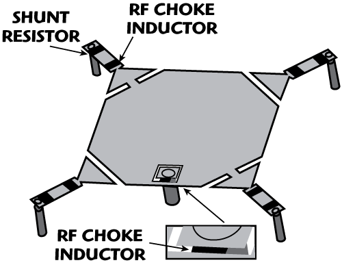
Figure 3 Antenna model used in the HFSS simulation including bias components.

Figure 4 Simulated results for the antenna model with and without bias network.
The fabricated prototypes are shown in Figure 5. Following F. Yang and Y. Rahmat-Samii,8 the PIN-diode switch is treated as an ideal model in the prototypes. That is, when the switch is in the off-state, it is removed from the patch, and when the switch is in the on-state, it is modeled as a metal pad. Return losses of the antenna prototypes are measured with an Agilent 8722ES network analyzer. The far-field radiation patterns are measured in an anechoic chamber. Because the structure is symmetrical for the CP states, RHCP results are sufficient to show the CP radiation properties.
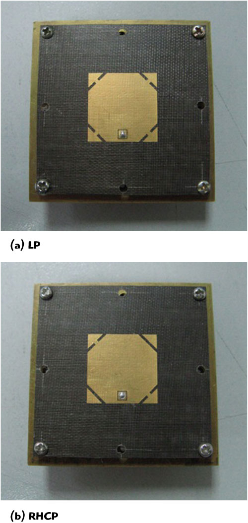
Figure 5 Photographs of the fabricated antenna prototypes.
Simulated and measured return losses are shown in Figure 6. The measured 10 dB impedance bandwidth for the LP state is 350 MHz, ranging from 5.19 to 5.54 GHz. The measured 10 dB impedance bandwidth for the CP state is 1380 MHz, ranging from 5.36 to 6.74 GHz. Figure 7 shows the simulated and measured results of the AR of the proposed antenna in the CP state. The best broadside AR of 0.824 dB is observed at 6.20 GHz. The associated AR bandwidth for less than 3 dB is 250 MHz, ranging from 6.08 to 6.33 GHz. Figure 8 shows the measured radiation patterns of the co-polarization and cross-polarization of the E-plane and H-plane for the LP state at 5.3 GHz. The measured linear spinning pattern of the CP state at 6.2 GHz in the yz-plane is also shown. Similar radiation patterns are observed in the xz-plane. An AR of less than 3 dB is achieved within a 60° beam width.

Figure 6 Simulated and measured return losses.

Figure 7 Simulated and measured AR vs. frequency.
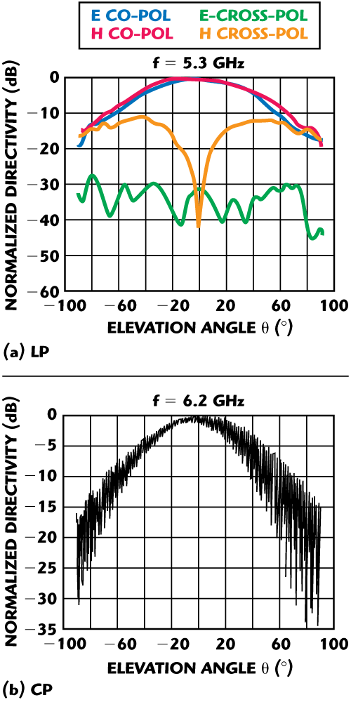
Figure 8 Measured radiation patterns of the proposed antenna.
Conclusion
A novel reconfigurable antenna with both frequency and polarization diversities is proposed. Using four PIN-diode switches on a square patch, the antenna can be operated either in an LP state or in a pair of orthogonal CP states at two distinct frequency bands. The frequency bandwidths are improved by using a capacitive gap. Experimental results show that good performance is achieved. This novel antenna can be a good candidate for future frequency and polarization diversity applications in wireless communication systems.
Acknowledgments
This work is supported by the Microwave and Millimeter Wave Engineering Research Center at the University of Science and Technology of China. The authors would like to thank Wang Xiaolu for the antenna measurements.
References
- J.T. Aberle, S.H. Oh, D.T. Auckland and S.D. Rogers, “Reconfigurable Antennas for Portable Wireless Devices,” IEEE Antennas and Propagation Magazine, Vol. 45, No. 6, December 2003, pp. 148-154.
- D. Peroulis, K. Sarabandi and L.P.B. Katehi, “Design of Reconfigurable Slot Antennas,” IEEE Transactions on Antennas and Propagation, Vol. 53, No. 2, February 2005, pp. 645-654.
- D.E. Anagnostou, G. Zheng, M.T. Chryssomallis, J.C. Lyke, G.E. Ponchak, J. Papapolymerou and C.G. Christodoulou, “Design, Fabrication and Measurements of an RF-MEMS-based Self-similar Reconfigurable Antenna,” IEEE Transactions on Antennas and Propagation, Vol. 54, No. 2, February 2006, pp. 422-432.
- Y.F. Wu, C.H. Wu, D.Y. Lai and F.C. Chen, “A Reconfigurable Quadri-polarization Diversity Aperture-coupled Patch Antenna,” IEEE Transactions on Antennas and Propagation, Vol. 55, No. 3, March 2007, pp. 1009-1012.
- H. Aïssat, L. Cirio, M. Grzeskowiak, J.M. Laheurte and O. Picon, “Reconfigurable Circularly Polarized Antenna for Short-range Communication Systems,” IEEE Transactions on Microwave Theory and Techniques, Vol. 54, No. 6, June 2006, pp. 2856-2863.
- N. Jin, F. Yang and Y. Rahmat-Samii, “A Novel Patch Antenna with Switchable Slot (PASS): Dual-frequency Operation with Reversed Circular Polarizations,” IEEE Transactions on Antennas and Propagation, Vol. 54, No. 3, March 2006, pp. 1031-1034.
- S.M. Kim and W.G. Yang, “Single Feed Wideband Circular Polarized Patch Antenna,” Electronics Letters, Vol. 43, No. 13, June 2007.
- F. Yang and Y. Rahmat-Samii, “Patch Antenna with Switchable Slot (PASS): Dual-frequency Operation,” Microwave and Optical Technology Letters, Vol. 31, No. 3, November 2001, pp. 165-168.