
Wireless technologies have developed in a way that can best be described as ‘unbelievable.’ Global mobile subscriptions rose to 1.7 billion in 2004 and the number continues to grow at a healthy pace. Furthermore, the production volumes of cellular phones are remarkable when compared to other consumer products — by 2002 the number of cellular phones sold worldwide was more than double that of the combined number of vehicles and PCs.
The interest in the evolution of cellular phones nowadays is focused mainly on the applications. The cellular phone, the main device that people always carry with them, is considered the key platform for mobile convergence applications, including web browsing, imaging, high bit-rate video streaming and video calls. With convergence, cellular phones will evolve from the traditional cost-optimized handhelds to multifunctional interoperable terminals in a variety of form-factors. The applications, together with the cellular phone form-factor, design and user interface, provide the main means of differentiation among manufacturers.
The transceiver side, on the other hand, has long been driven by the increased need for integration, cost-reduction and, to some extent, power reduction. Currently, transceiver development has reached a certain maturity, as shown by the block diagram of today’s typical, basic category triple-band GSM phone in Figure 1. The engine consists of three main chips: one for RF, one for baseband, and one for mixed-signal and energy management. The chips are either proprietary designs or based on available chip sets. The product includes a total of 345 parts. While integration, cost and power reduction are still key challenges for cellular phone development, it is the number of additional radios that explode the complexity of the transceiver.

Fig. 1 Block diagram of a typical ceccular phone.
The objective of this article is to discuss the key challenges of transceiver implementation for future mobile terminals. The architecture development and opportunities for further integration are described and the key challenges of the multiradio concept driven by various radio standards are presented. Finally, strategies for managing the growing complexity are discussed.
Past Architecture Development
New implementation architectures enable the adoption of new technologies. The new technologies, in turn, bring improvements in product requirements, such as performance, miniaturization, power consumption, reliability and cost. In wireless access implementation, several successful development steps over the last 15 years of cellular phone development have laid the foundation for future technology advances. These steps have provided clear improvements in miniaturization and functionality, as shown in the wiring board-level engine development illustrated in Figure 2. In the first phase, the RF and baseband circuitry were implemented on separate printed wiring boards (PWB). Careful design of the wiring board and shieldings enabled the embedding of the whole engine on the same wiring board, resulting in a significant size and cost reduction of the cellular phones. The market saw the first real handportable devices.

Fig. 2 Engine development for ceccular phones.
The next major step was the integration that took place within both the baseband and RF. Digital signal processing (DSP) and microprocessor unit (MPU) functionalities were integrated together with logic circuitry on a baseband application-specific integrated circuit (ASIC). In the RF side, the discrete superheterodyne RF was mapped onto silicon RFICs. Again, significant size and cost benefits were achieved.
In the RF front-end, however, it was the next architecture, the direct conversion, which really benefited from the silicon implementation. Although the direct conversion receiver architecture is old, it was not feasible for mass-production for a long time because of DC offset and signal self-mixing problems. The architecture became practical only in the mid-1990s when RFIC technology had matured to include sufficiently fast and homogeneous transistors, and the quality of the design models and tools had improved significantly.
Direct conversion architecture provided huge benefits in component count reduction; several filters and synthesizers were removed and the total silicon area was reduced. Furthermore, when multi-band and 2G/3G multi-mode transceivers became a requirement, the direct conversion architecture proved to be a flexible platform for the multi-mode operation enabling easy reuse of several functional blocks.
Impact of CMOS Evolution
Looking to the future of RF, digital CMOS technology has been the hottest research topic in recent years. The 130 nm bulk CMOS technology has also proven to be applicable for the RF, but it still suffers from several disadvantages. In particular, substrate-coupling effects are stronger and the maturity of transistor models is not at a comparable level as in the widely used RF BiCMOS. With 90 nm and 65 nm technology nodes, physical effects, such as leakage currents and process variations, start to have a significant impact on performance.1 Furthermore, the cost calculation of RF CMOS reveals that a one-to-one replacement of the RF circuit with a CMOS version provides only marginal, if any, cost benefit. The calculation changes immediately when large digital content, such as digital filtering and control logic, is integrated on the same chip.
To fully exploit the speed of the latest digital CMOS technology in RF, new circuits and architectures need to be invented. In contrast to just mapping the traditional RF circuits to CMOS, the new architectures could be based on fast sampling and time-discrete signal processing. The interface between the RF and baseband then becomes blurred and the portability of the RF front-end to the future CMOS process nodes improves dramatically. Recently, examples of new, more digital architectures have been reported.2,3 These new architectures pave the way to true single-chip radios, especially for products for high volume entry markets.
In the baseband, the processing power requirement and the complexity continue to grow with high data rates. Today, the baseband ASICs that include the processor core or cores are not only limited in performance by the computational power, but also by the on-chip communication, line delays and clock distribution. In order to reduce the load from the processing cores, decentralized architectures are being considered. Small controller processors or units running at low frequencies can then be distributed within the engine. With multiple processors, management of the processing power resources becomes one of the key challenges.
An alternative approach to optimize the baseband is to utilize configurable logic, configurable processors or processor generators. They provide more freedom in optimizing the trade-off between performance and flexibility. Still, due to the exploding baseband complexity of cellular platforms, the main challenges have to do with design methodology, verification and testability.
Multiradio
The evolution of wireless standards is not showing any signs of convergence towards a small number of global systems. Instead, the current wireless systems continue to evolve and new systems are being proposed and put into use for consumer applications. The cellular wireless systems will adopt higher data rates — high speed downlink packet access (HSDPA), the evolution of the WCDMA system, will offer, in the first phases, average data speeds of 1 to 2 Mbit/s, which in subsequent phases will increase to over 10 Mbit/s.
In addition to cellular systems, other wireless systems start to find their way into mobile terminals, including proximity radios (Bluetooth and RFID, for example), wireless local area network radios (IEEE802.11a/b/g), and receivers for positioning (GPS) and broadcasting (DVB-H). Wireless broadband offering fast wireless Internet access with good coverage and mobility is likely to become yet another category of radios. Although some radios are serving a clearly identified application, such as GPS for positioning, many applications will be available through different radio bearers. Thus, the services are required to be radio-agnostic in the multiradio environment. This is best achieved by utilizing the Internet protocol convergence as the unified connection layer.
The high number of radios introduces huge challenges for the terminal implementation, as shown in Figure 3. The transceiver part of the mobile terminal is developing towards versatile multiradios with a large number of parallel functional blocks that can interfere with each other. The interference tolerance from several concurrently operated radios becomes a requirement that exceeds the specifications in the radio standards. The optimized integration level, on the other hand, depends on the variety of product variants based on the same platform. Architecture modularity then becomes a key target for rapid product development. Furthermore, reconfigurability and reuse of circuit blocks can be a means for complexity and silicon area reduction in multiradio implementation.

Fig. 3 Multiradio components
Multiradios introduce miniaturization challenges to the antennas and front-end filters. More than ten different antennas is unacceptable from a volume utilization perspective. Instead, the antennas need to be designed as compact multi-system antenna modules and filter miniaturization is crucial. Bulk-acoustic-wave technology (BAW) is one key enabler for filter miniaturization whereas micro-electro-mechanical systems (MEMS) technology still requires proof for RF applications.
Strategies for Complexity Management
The evolution of communication and application functions has substantially increased the system level complexity — the number of functional blocks increases, resulting in a growing number of interfaces, power consumption increases, and the amount of data increases, resulting in growth in traffic and memory space. Methods and technologies to tackle the increasing complexity of the system include standardized solutions and interfaces, adaptive and flexible platforms, and more accurate modeling.
The key interfaces of cellular engines, as shown in Figure 1, for example, have traditionally been based on dedicated solutions. As the variety of components that can be used to build the products in the future, especially in the more high end categories, will significantly grow, it will not be possible to go on with only dedicated implementations. Interfaces need to be standardized to easily attach new components to the system. The Mobile Industry Processor Interface (MIPI) alliance is an example initiative for standardized interfaces for mobile application processors.4
To achieve the best performance in handheld devices, any overhead in the system must be eliminated; therefore, adaptive solutions are required, such as dynamic voltage and frequency scaling, and the usage of reconfigurable circuits in baseband platforms. All possible means for preventing unnecessary switching in digital circuits and overheads in latencies need to be applied. Flexibility will be the key enabler to implement a wide selection of product categories in the future. As a part of this strategy, enormous ASICs may not be the most probable choice, because they can be too expensive and more difficult to test. In addition to flexibility, power consumption, total cost and time-to-market continue to be important drivers.
Tying Everything Together with Design Tools
As complex systems comprise an enormous amount of parameters and dependences to be optimized, advanced electronic design automation (EDA) tools are needed to support product development. Tools are enablers for faster time-to-market and boosters of evolution. Achievements in embedding, miniaturization, power savings or design verification depend strongly on the tools. The top-down design flows currently available still have weak spots that require extensive effort and orientation from the designers.
Today’s multilevel requirements include C-code, very high speed IC description language (VHDL) and transistor-level descriptions, not only traditional mixed-signal based environments. A better framework and standardized data transmission formats are needed for information transfer from one tool to another and to fully enable utilization of intellectual property blocks in integrated circuit design.
Closer collaboration between technology and EDA tool houses is needed to provide seamless, reliable and tested design environments. Tool integration challenges are visible in particular in substrate noise modeling tools, 3D package modeling combined with RFIC simulations, HW/SW partitioning optimization, and more powerful and flexible antenna simulation algorithms, and in adding RF imperfections into system simulations.
Tight Power Budget
Since the middle of the 1990s, many 2G phones have provided users with good operation times. As an example, the first member of the Nokia 6000 cellular phone series introduced in 1997 provided 3.3 hours of talk-time and 180 hours of standby time. Using that as a reference and focusing on talk or application times, the general trends in power consumption and lithium-ion battery capacity can be represented, as shown in Figure 4. Constant annual growth of approximately 10 percent in battery capacity has enabled continuous battery volume shrinkage, while having the absolute milliamperehour level constant over the years. It has also enabled new features like multislot transmission in a GSM uplink without significant compromises in operation time. Figure 4 describes the highest output power levels in the transmitter, which in real life happens only very infrequently. Most of the time, the total power consumption is significantly lower. The good news is that technology evolution has also enabled good talk-time for the first WCDMA phones, even at the maximum transmitter power level. However, careful design is needed for the highest power consumption peaks, when 3G or WLAN communication is run simultaneously with multimedia applications. Therefore, it is important that the power consumption of the wireless access engines be reduced in the future to release power for the applications.
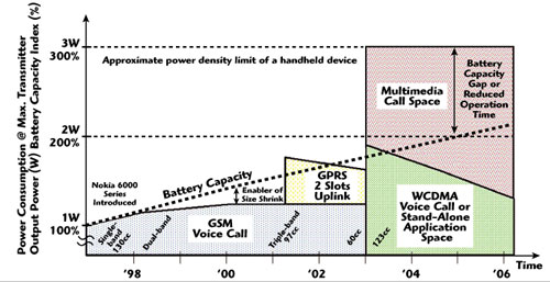
Fig. 4 Battery capacity and power consumption indexes with the maximum output power level in cellular transmitters.
The power partitioning in a 3G phone is represented in Figure 5. Power consumption can be divided into four significant portions: transmitter, including the power amplifier, receiver, digital and mixed-signal ASICs, and user interface HW, including the display, speaker, etc. Compared to the power partitioning in a 3G terminal, the power amplifier more noticeably dominates the power consumption in 2G terminals. Typical power-added efficiencies of the GSM power amplifiers are in the range of 40 to 55 percent.
 |
| Fig. 5 Power consumption breakdown in video streaming in a 3G phone. |
In WCDMA, a non-constant envelope modulation is used; therefore, the power amplifier has to operate in linear mode, resulting in lower power-added efficiencies — typically in the range of 30 to 40 percent. Since the transmitters are rarely used at the maximum power level in cellular systems, not only should the maximum efficiencies be compared, but the overall power consumption over the probability-density function of the transmitted power of the terminal should be evaluated.
Conclusion
Mobile phones are complex embedded systems where all functional blocks are custom-made for mobility. The combination of miniaturization and functionality is unprecedented compared to other consumer products. In terms of production volumes, the mobile phone is in a class of its own. Development has been based on advances, either evolutionary or disruptive, in implementation architectures and technologies. In particular, mobile phones have benefited from the early exploitation of leading-edge semiconductor technologies. With the rapid growth of the number of radios that are taken into use in mobile terminals, the architectures and technologies of wireless access continue to be optimized towards versatile multiradios.
The multiradios bring huge challenges to transceiver architecture, interference tolerance and miniaturization. The evolution of system complexity is taking a large step forward; consequently, system complexity management becomes the main challenge. To meet the time-to-market requirements while applying new technologies and techniques, advanced system level design tools are needed. In particular, power consumption, top-down design flow, flexibility, HW reconfigurability, programmability, standard interfaces and embedding are the key features that should be mastered in advanced system level design tools.
Acknowledgments
The author would like to thank Yrjö Neuvo and Mika Tiilikainen for their contributions to this article.
References
1. J.A. Croon, S. Decoutere, W. Sansen and H.E. Maes, “Physical Modeling and Prediction of the Matching Properties of MOSFETs,” Proceedings of the European Solid-State Device Research Conference 2004.
2. R. Staszewski, J. Wallberg, S. Rezeq, C.M. Hung, O. Eliezer, S. Vemulapalli, N. Barton, M.C. Lee, P. Cruise, C. Fernando, M. Entezari, R. Staszewski, K. Maggio, K. Muhammad and D. Leipold, “All-digital PLL and GSM/EDGE Transmitter in 90 nm CMOS,” Digest of Technical Papers of Solid-State Circuits Conference 2005.
3. P. Eloranta and P. Seppinen, “Direct-digital RF Modulator IC in 0.13 µm CMOS for Wideband Multi-radio Applications,” Digest of Technical Papers of Solid-State Circuits Conference 2005.
4. www.mipi.org.
Petteri Alinikula received his MSc degree in electrical engineering from the Helsinki University of Technology, Espoo, Finland, in 1988, and his PhD degree from Pennsylvania State University, University Park, PA, in 1992. From 1992 to 1993, he was the head of the Microelectronic Center, IC Design Unit, Helsinki University of Technology. In 1993, he joined the Nokia Research Center, Helsinki, Finland, where he is currently senior research manager, responsible for radio integration research.