
An overview of the 28-42-50 V LDMOS technologies is given and the ruggedness reliability is discussed, in addition to the RF performance. Various ruggedness tests are presented such as pulsed snapback measurements, VSWR and video bandwidth tests.
RF power amplifiers are key components in base stations, broadcast transmitters, ISM applications and microwave applications. They can handle a wide range of signal types such as GSM, EDGE, W-CDMA, WiMAX and DVB-T. RF laterally diffused MOS (LDMOS) transistors have been the technology of choice for these power amplifiers for more than a decade, because of their excellent power capabilities, gain, efficiency, cost and reliability.
Ruggedness is one of the most important reliability parameters for RF power transistors. Ruggedness is the ability to withstand a stress condition without degradation or failure. One way to characterize ruggedness is by measuring the voltage standing wave ratio (VSWR) in an RF test fixture with a defined mismatch at the output. The design of the test fixture and the matching of the transistor are critical for the result of the VSWR test. LDMOS transistors are optimized to withstand a certain power and voltage, and the process is engineered for the best trade-off between RF performance and ruggedness.
In this article, RF LDMOS devices are shown, which combine very good ruggedness with state-of-the-art RF performance. Ruggedness tests, which have been developed to meet today’s product ruggedness criteria, will be described.
RF LDMOS Technologies (28-42-50 V)
NXP Semiconductors has developed a base station RF LDMOS technology1,2 and high voltage RF LDMOS technologies.3 The base station technology operates at supply voltages of approximately 28 V, while the high voltage technology can be used at 42 and 50 V. Both LDMOS types are processed in an 8-inch CMOS-fabrication environment, capable of lithography down to 0.14 mm, where the LDMOS process is derived from the C075 CMOS (0.35 μm gate) process with LOCOS isolation. Additions to this C075 process are the source sinker to the substrate, CoSi2 gate silicidation, tungsten shield and mushroom-type drain structure with thick multi-layer AlCu metallization. A schematic picture of the LDMOS is shown in Figure 1, where the inherently present NPN parasitic bipolar transistor is indicated by the red rectangle.

Figure 1 Schematic picture of LDMOS technology.
The RF performance of the base station LDMOS is state-of-the-art and is used in a wide range of applications like GSM, W-CDMA and WiMAX.1 Recently, high voltage (42 to 50 V) LDMOS technologies3 have been developed for high power devices at frequencies below 1 GHz. Typical RF performance of the high voltage technology at 470 to 860 MHz (UHF) and 225 MHz (VHF) is shown in Figures 2 and 3, respectively. The UHF device delivers 75 to 110 Wavg at 42 and 50 V, respectively. The broadband gain is 19 dB and the efficiency is 30 to 32 percent with a Complementary Cumulative Distribution Function (CCDF) of 8 dB. The VHF device delivers 1300 W power (P1dB) at 50 V with a peak efficiency of over 70 percent and a gain of 24 dB.

Figure 2 RF performance of the 42 V and 50 V LDMOS technology devices at 470 to 860 MHz for an 8k DVB-T signal.

Figure 3 RF performance of a 50 V LDMOS device (BLF-578) at 225 MHz.
Both devices have been tested to be very rugged and capable of handling high voltage and high power over a wide band of extreme mismatch conditions. In general, at low frequencies, more ruggedness is required of devices. This is partly due to the higher harmonic content at frequencies much lower than the cut-off frequency. Also, the signal type is important for ruggedness, sharply varying pulse signals with a steep rise time being more severe for ruggedness. For this reason, LDMOS technologies have been hardened under the most stringent ruggedness tests during development, and in particular the 50 V high voltage technology.
Parasitic Bipolar Transistor
Inherent to the LDMOS device is the presence of a parasitic bipolar transistor. This NPN bipolar transistor is indicated in the schematic picture of the device. The corresponding electrical schematic is given in Figure 4, showing, in addition to the LDMOS, the presence of the parasitic NPN bipolar transistor and the drain-substrate diode. The drain-source diode clamps the voltage across the LDMOS and the parasitic bipolar and sinks the excess current to the substrate. For large sink currents, however, the drain-source voltage exceeds the diode breakdown voltage and the parasitic bipolar transistor can be triggered.

Figure 4 Electrical representation of the LDMOS and the inherently present parasitic bipolar transistor and drain-substrate diode.
This triggering of the parasitic bipolar transistor is essential for the occurrence of a ruggedness failure. To make the bipolar transistor robust for a triggering event, the bipolar of the LDMOS has been characterized and optimized. Important transistor parameters for triggering are the base resistance (RB), the gain of the bipolar and the amplitude of the base current. As a characterization tool for the triggering of this bipolar, a short pulse (50 to 200 ns) is used in the measurement of the current-voltage characteristics. An impedance transmission line is used as a pulse source to create a rectangular pulse. The desired voltage is applied via a DC power supply and then quickly discharged with a low inductance switch. The current and voltage are measured with a memory scope during the discharge. The snapback in the I-V curve is measured, which gives insight in the device properties of the DUT. The characterization is done on a wafer with small (test) devices in a 50 Ω commercially available set-up. Power RF devices cannot be used, since the setup is not able to generate enough current. This is a fast and adequate evaluation of device and process changes on ruggedness without the influence of test circuits and matching conditions.
Ruggedness Characterization
During the development of RF-LDMOS processes, the intrinsic ruggedness of the parasitic bipolar transistor of the RF power LDMOS devices has been continuously improved.
The base resistance is important for ruggedness as can be seen from the electrical representation of the LDMOS. In the processing, the base resistance of the parasitic bipolar transistor has been varied to lower the voltage drop between base and emitter. In Figure 5, the pulsed current-voltage characteristic of base station RF LDMOS devices is shown for different base resistances. Around the (diode) breakdown voltage of the transistor (in this example at approximately 73 V), the drain current starts to increase and at 82 V a snapback occurs. This snapback voltage and snapback current are the two parameters that are a measure for the intrinsic RF ruggedness. By process optimizing the base resistance, the snapback current has been successfully doubled, resulting in a better VSWR of the corresponding power devices.

Figure 5 Pulsed current voltage characterization of several devices with different base resistance.
Furthermore, the capacitance between the base of the bipolar and the drain (CDB) has been optimized by engineering the drain extension of the LDMOS. Figure 6 shows measurements for different drain engineering (DE) variants. At 83 to 98 V, the parasitic bipolar of the device is triggered, causing a snapback in the curve. This snapback is improved by DE variation, resulting in a more rugged device. This is confirmed by VSWR measurements done on power devices. The best devices can tolerate a 10 V higher supply voltage for the same power level and a VSWR of 10:1.

Figure 6 Characterization of devices with different drain engineering variants at Vgs = 0 V.

Figure 7 Pulsed current-voltage measurements of the high-voltage broadcast LDMOS for different epi thickness.
From this rugged base station LDMOS technology, a super-rugged high voltage (42 to 50 V) RF LDMOS technology has been derived for broadcast applications up to 1 GHz and for VHF and ISM applications, where the most stringent reliability criteria are demanded. Figure 7 shows that the breakdown voltage of these high voltage technologies is increased, compared to the 28 V base station technology. More importantly, the snapback voltage is also significantly larger, resulting in values of 130 and 150 V. Simultaneously, the snapback current is more than doubled compared to the base station technology, shown previously. High voltage power devices have been measured for a VSWR of 10:1 at the nominal supply voltage of 42 to 50 V, but they can even withstand values up to 60 to 70 V, as expected from the figure. This ruggedness has been achieved by engineering of the drain extension, epi layer thickness and shield construction.
From the snapback current and voltage, the maximum dissipated power before failure is calculated. This power is an indication for the quality of the ruggedness of a power device, as shown in Figure 8 for 42 V development devices. The power at which a power device fails (applying a VSWR of 10:1 with a DVB-T signal) is plotted versus the power at which an on-wafer test device fails (pulsed current voltage sweep). A linear relation is found between the power and on-wafer test device, which indicates this on-wafer test is a good predictor for the ruggedness of a power device. For large powers, there is a deviation from the linear trend. It is speculated that this is due to thermal aspects and circuitry matching.
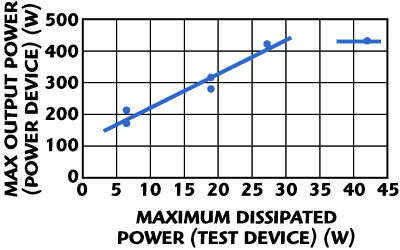
Figure 8 Correlation between the peak power at which a power device fails (VSWR = 10:1, 8k DVB-T, 9.5dB PAR) and the power dissipated at snapback of a corresponding test device.
Ruggedness Safe Operation Area
In the application, not only a drain voltage is applied but also a gate voltage. If the applied gate voltage is above the threshold voltage, a current will flow in the transistor and in the base. This base current in combination with a high drain voltage will more easily trigger the parasitic bipolar transistor. The failures of devices have been measured for a wide range of current-voltage settings to construct a parasitic bipolar safe operation area (PB-SOA). The constructed PB-SOA curve is shown in Figure 9.

Figure 9 Constructed safe operation area of the parasitic bipolar transistor as derived from on-wafer pulsed I-V measurements for NXP base station RF LDMOS.

Figure 10 Schematic picture of the safe operation area.
This PB-SOA curve resembles the theoretical safe operation area curve (see Figure 10), as is known for CMOS devices for instance. A few I-V characteristics and the class AB load line have been added.
The load line approached the edge of the SOA at its two extremes: at high drain current and at high drain voltage. For high current, the triggering of the bipolar is thermally induced, while at high drain voltage the triggering is electrically induced. By engineering the snapback characteristic, the LDMOS devices are optimized to prevent the occurrence of the electrically induced triggering, since this mechanism is the most frequent cause for ruggedness failures, as determined from the occurrence of a random damage pattern. Also, the thermal behavior of LDMOS is part of the continuous improvement.
Ruggedness in Applications
After the on-wafer pulsed current voltage ruggedness measurements, several ruggedness tests are performed in the application circuitry, the most common one being a measurement of the VSWR. In data sheets, a VSWR of 10:1 is typically specified under nominal power conditions.
A wider bandwidth operation is required for more complex signals like W-CDMA. This puts heavier constraints to the broadband decoupling of circuits. The LDMOS device has to withstand signal deformations due to a non-ideal decoupling. To test the wideband ruggedness, a video bandwidth (VBW) measurement is performed. In a VBW test, a signal with 2 tones in compression is applied, with a tone spacing of Δf. The tone spacing is increased until the device fails. Such a VBW test is shown in Table 1 for the base station LDMOS technology with a Δf of 80 MHz. This is a typical bandwidth for multi-slot W-CDMA amplifiers. Usually the LDMOS is operated at 32 V, but the devices pass up to 35 V supply voltage with this 80 MHz tone spacing as shown in the table.

Table 1 VBW Measurement at Various Supply Voltages Around a Center Frequency of 2 GHz for a Tone Spacing of 80 MHz. POUT is the Power for a Single Tone
Extremely rugged devices are in the high voltage technology families. These devices operate at 42 to 50 V at UHF or VHF frequencies, low frequencies where the most ruggedness demands exist. In Figure 11, the VSWR versus output power is plotted for drain supplies of 50 and 55 V applied to a BLF578 device for a signal at 225 MHz with a 20 percent duty cycle. As predicted by the on-wafer tests (discussed in the ruggedness characterization section), the device can easily tolerate 55 V drain voltage in combination with a VSWR of 20 and a power of 1.4 kW, values far above the nominal operation settings.

Figure 11 VSWR ruggedness measurement at various output power for a pulsed CW (with 20% duty cycle) signal at 225 MHz.
Conclusion
Various ruggedness reliability tests have been described for RF power transistors. Pulsed on-wafer snapback measurements during the development and VSWR and video bandwidth tests in the application circuitry are used to optimize the ruggedness of 28-42-50 V LDMOS technologies. Extremely rugged devices have been developed in combination with state-of-the-art RF performance.
Acknowledgments
The authors wish to acknowledge J. Gajadharsing, B. Merkus, H. Mollee, P. Hammes, T. Bakker, K. Vennema, J. Klappe and M. Murphy for all discussions and support during the development.
References
- F. van Rijs and S.J.C.H. Theeuwen, “Efficiency Improvement of LDMOS Transistors for Base Stations: Towards the Theoretical Limit,” 2006 International Electron Devices Meeting Digest, pp. 205-208.
- S.J.C.H. Theeuwen and H. Mollee, “LDMOS Transistors in Power Microwave Applications,” December 2008 White Paper at Microwave Journal website, http://www.mwjournal.com/search/article.asp?HH_ID=AR_6871.
- S.J.C.H. Theeuwen, W.J.A.M. Sneijers, J.G.E. Klappe and J.A.M. de Boet, “High Voltage RF LDMOS Technology for Broadcast Applications,” Proceedings of the Third European Microwave Integrated Circuits Conference, 2008, EuMIC02-2, pp. 24-27.