
 RF performance and thermal reliability are the two important parameters when selecting an RF Tx/Rx switch at the front end of a high power linear base station, CPE, or femtocell. As always, the RF performance is very critical. Parameters such as insertion loss, isolation, P1dB, IP3, switching speed, bandwidth and VSWR are important to the system designer. These linear systems exceed power levels beyond 10 W of average power, which pushes the designer to consider the switch’s thermal properties early in the decision making process. For example, a 10 W signal incident on a switch with 1 dB of insertion loss at 3.5 GHz will require the switch to handle 2 W of power dissipation. The maximum junction temperature of the device could be violated and the lifetime reliability of the component could be compromised if this isn’t taken into consideration. The fundamental limitation of power handling at any frequency is ultimately thermal. This is true for both long-term reliability and short-term catastrophic failures.
Linear TDMA systems such as WiMAX and TD-SCDMA use modulation schemes that create very high peak-to-average ratios on the RF power signal. This ratio can be as high as 12 dB specifically for WiMAX systems. This needs to be considered for both the linear performance of the switch as well as the thermal reliability. The 1 dB compression point (P1dB) of a switch only provides a rough guideline as to the true linearity of the switch in this type of linear system. The delta between the switch’s P1dB and its Error Vector Magnitude (EVM) at 1 percent can be anywhere between 8 and 12 dB depending on the topology of the switch.
Critical parameters for a higher power Tx/Rx switch include lower insertion loss, especially on the Tx path in order to minimize the requirements of the power amplifier. High isolation in the switch is just as critical since excess leakage from Tx to Rx will saturate the LNA. M/A-COM Technology Solutions has developed a monolithic PIN diode-based SPDT, the MASW-000834-13560T, on its Heterolithic Microwave Integrated Circuit (HMIC) technology to address both the RF and thermal needs of these linear systems. HMIC is the ultimate form of SOI, which has a unique thermal design that provides the ability to both handle > 1000 W of pulsed peak and up to 50 W of CW RF incident transmit power, while simultaneously providing very low RF distortion, excellent linearity and high receive isolation. This results in high performance devices that are not available with other traditional processes.
HMIC is a unique process that combines glass and silicon that enables the high frequency and high power handling properties of the two materials to be optimized plus provides true surface-mount device structures to be produced using standard semiconductor processing equipment and techniques. It also allows for the integration of high Q (or low loss) passives as well as low Rs (series resistance) active elements in order to create more complex components. This allows for smaller size components like the MASW-000834-13560T with low loss and high power handling. In addition, the monolithic insertion of various diode-based active components such as PIN diodes and Schottky diodes in the HMIC circuit topology allows a number of more complex monolithic integrated circuits to be realized.

Figure 1 Cross-section of the HMIC device.
A cross-section for both passive and diode-based HMIC devices is shown in Figure 1, which shows the elements needed for HMIC circuit design. Silicon vias to achieve vertical connections (i.e. front to back) are a natural consequence of the HMIC fabrication process. The top surface of these vias typically serves as the “active” layer for the formation of the required diode-based active devices and as possible interconnection paths for the requisite passive elements. The various circuit elements, either active or passive, are then laterally linked using standard photolithography and metallization techniques.
The shunt diode has the highest power handling since it has a very high thermal conductivity from the surface to ground. The series diode, by contrast, is always the weaker thermal link in the design since it has the lowest thermal conductivity. The thermal analysis needs to focus on improving the thermal properties of the series diode in order to increase its power handling capacity. Although the series diode is electrically in series, it needs to focus on its thermal shunt cross-section. One area specifically focused on is the insulating epoxy under the series diode. Optimizing the thickness of the boron filled, electrically insulating thermal epoxy between the cathode and bottom metallization offers the best compromise between electrical insulator, thermal conductivity and manufacturability, which M/A-COM Technology Solutions has optimized over many years of experience.

Figure 2 MASW-000834-13560T broadband performance.
HMIC allows for broader band operating frequency and lower parasitics while operating at high power levels than traditional devices, as shown in Figure 2. For instance, the MASW-000834-13560T achieves 0.3 dB insertion loss and over 40 dB of Rx isolation at 2.5 GHz while handling power levels up to 50 W of CW power without degradation of the basic PIN diode junction parametric characteristics.
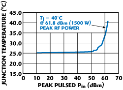
Figure 3 MASW-000834-13560T junction temperature vs. peak pulsed input power (50 μsec pulse width, 1% duty cycle).
In terms of the pulsed Tx power handling, the use of the boron filled epoxy, larger vertically etched silicon pedestals, and optimized anode topology design allows for significant power handling, as shown in Figure 3, which is a plot of measured junction temperature versus pulsed input power at 50 μsec pulse widths and at a 1 percent duty cycle. A peak incident power level of +61.8 dBm, approximately 1500 W, in the Tx mode results in a junction temperature of 40°C, which is a 15°C rise over ambient, and well below a safe maximum operating temperature of 175°C.

Figure 4 MASW-000834-13560T junction temperature vs. CW input power.
When the Tx arm of the MASW-000834-13560T SPDT is operated in CW mode, Figure 4 shows that a maximum safe junction temperature of 175°C is reached at an incident drive level of +46.8 dBm or 47.8 W at an ambient heat sink temperature of 25°C. This HMIC design out performs other traditional designs by a wide margin and can be used in commercial and military applications.
Conclusion
M/A-COM Technology Solutions has developed a high power PIN diode-based Tx/Rx switch, the MASW-000834-13560T, capable of simultaneously delivering broadband performance (DC to 6 GHz) while reliably handling high power levels utilizing the patented HMIC integration technology. This technology has the ability to produce low loss series PIN diodes that have both high electrical isolation from the ground plane and a low thermal impedance to maintain reliable peak junction temperatures that out performs traditional devices currently available in the market.
M/A-COM Technology
Solutions Inc., Lowell, MA
(978) 442-5000,
www.macom.com.
RS No. 301