
InP-based heterojunction bipolar transistors (HBT) have shown excellent microwave and noise performance and are very attractive for millimeter-wave and optoelectronic applications, such as low noise amplifiers (LNA), mixers, oscillators and other RF sub-system components. HBTs are almost exclusively operated in a common emitter configuration (CE) in amplifier design. However, a common base configuration (CB) has the advantages of ease of broadband impedance matching with a better gain and is more suitable for optical and microwave broadband communication applications.1-4 At the same time, the common collector configuration (CC) has been widely used as an isolator and buffer in microwave monolithic integrated circuits.5
A complete characterization of the transistor (CE, CB and CC) in terms of noise and scattering parameters is necessary for the computer-aided design (CAD) of microwave circuits. The S- and noise-parameters for each configuration can be obtained by measuring the test patterns of CE, CB and CC configurations. However, this method requires two special test structures (CB and CC) for each device size on the wafer, and the non-uniformity across the wafer has to be ignored. Alternatively, analytical expressions for the relationships between common emitter, common base and common collector HBTs are very attractive and useful for understanding the relation between the different configurations. The direct transformation technique for microwave FET devices has been discussed in more detail previously.6-8 However, a comprehensive analytical expression for the different HBT configurations has not yet been published.
In this article, a simple but efficient transformation technique for microwave HBT devices is proposed. This technique is based on the combination of an equivalent circuit model and a conventional two-port network signal/noise correlation matrix technique. The signal and noise parameters of the CB and CC configurations can be obtained directly by using a simple set of formulas from the CE signal and noise parameters. All the relationships provide a bi-directional bridge for the transformation between CE, CB and CC HBTs, respectively.
Theoretical Analysis
Small-signal Model

Figure 1 Small-signal equivalent circuit model in CE configuration.
The conventional hybrid-T type small-signal equivalent circuit model in the CE configuration is shown in Figure 1. Since the T-shaped equivalent circuit is more closely related to the original derivation of the common base Y parameters of bipolar transistors, and involves less simplifying assumption than the π equivalent circuit, it is usually employed in the literature for the purpose of small-signal parameter extraction of HBTs. The circuit is divided into two parts, that is the outer part containing the extrinsic elements, considered as bias independent, and the inner part containing the intrinsic elements, considered as bias dependent.
In the small-signal equivalent circuit model, Cpi, Cpo and Cpio represent the pad capacitances, Lb, Lc and Le represent the inductances of the base, collector and emitter feed lines, Rbx and Rbi are the extrinsic and intrinsic base resistances, Rc and Re are the collector and emitter resistances, Cex is the extrinsic base-collector capacitance, and Cbe and Cbc are the intrinsic base-emitter and base-collector capacitances, respectively. It is noted that the extrinsic base-collector resistance Rex is neglected in this model, because the value of Rex is very large and does not affect the frequency response as long as only forward operation is concerned with.
The short circuit Y-parameters for the intrinsic part of the small-signal equivalent circuit in the CE configuration can be expressed as:

with

Assuming a single-pole appoximation, the transport factor can be written:
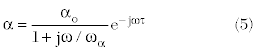
α0 denotes the intrinsic current gain at low frequency, ωα is the 3 dB roll-off frequency and τ is the transit time delay.
The CB configuration for the HBT devices considered in the studies can be obtained from exchanging the base and emitter in the CE configuration, and the CC configuration can be obtained by exchanging the collector and emitter in the CE configuration. Because the pad capacitances are the same for the three configurations, all the transformation formulas in this article will not include the effect of pad capacitances. The measured S-parameters and noise parameters without pad capacitances are obtained after de-embedding the pad capacitances.
Signal Parameter Relationships
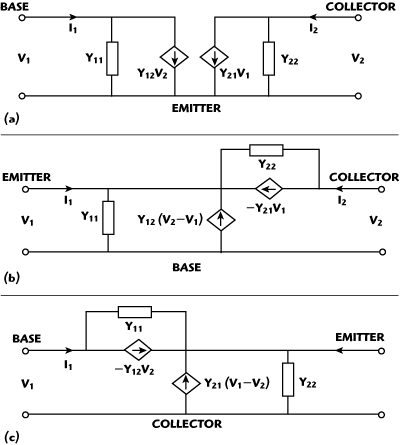
Figure 2 CS (a), CG (b) and CD (c) HBT configurations.
The equivalent two-port short circuit Y-parameters networks of the CE, CB and CC configurations for the HBT devices are shown in Figure 2. Comparing the Z-parameters of the CE, CB and CC configurations, the Y-parameter relationships can be obtained as follows:

Noise Parameter Relationships
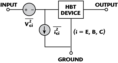
Figure 3 HBT noise equivalent circuit models for CE, CB and CC configurations.
Figure 3 shows the noise equivalent circuits of the CE, CB and CC configurations for HBT devices.  and
and  (i=E,B,C) are the two noise sources at the input of the noiseless HBT device for different configurations. The chain noise correlation matrix is easier to obtain from the noise measurement because there is a direct relation between the measured noise parameters (Fmin is the minimum noise figure, Rn the noise resistance, Gopt the optimum source conductance and Bopt the optimum source susceptance). The relationship of the noise parameters between the CE, CB and CC configurations can be obtained by using the noise source transformation matrix technique.6-8
The relationships between the CE and CB configuration are as follows:

where
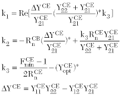
The relationships between the CE and CC configuration are as follows:

where

At the low frequency ranges (typically f < 6 GHz), the noise parameter relationships between the CE, CB and CC configurations for the intrinsic HBT device can be simplified by neglecting the influence of the parasitics:

Experimental Verification
In order to verify the equations derived in the theoretical analysis for the signal and noise parameters, InP/InGaAs DHBTs with a 5 x 5 µm2 emitter area have been characterized. The S-parameter measurements for model extraction and verification were made using an Agilent 8510C network analyzer. The DC bias was supplied by an Agilent 4156A. The microwave noise parameter measurements were carried out on the wafer over the frequency range from 1 to 20 GHz, using an ATN microwave noise measurement system NP5.

The extracted values of the extrinsic and intrinsic small-signal elements can be easily determined by using the direct extraction technique9,10 and are summarized in Appendix A. The bias condition is Vce=2.0 V and Ib= 50 µA (Ic=1.84 mA). An excellent agreement over the whole frequency range is obtained for the CE configuration.10 To illustrate the efficiency of the Y-parameter transformation formulas, the measured and predicted S-parameters for the CB and CC configurations are compared in Figures 4 and 5. Good agreement can be observed between the data calculated from the equivalent circuit model and the data predicted by the transformation formulas up to 40 GHz at a bias Ib=50 µA, VCE=2.0 V.

Figure 4 Comparison of modeled and predicted S-parameters for the HBT in CB configuration.

Figure 5 Comparison of modeled and predicted S-parameters for the InP HBT in CC configuration.
To illustrate the efficiency of the transformation formulas for noise parameters, the predicted and modeled results for InP HBT in the CB and CC configurations are compared in Figures 6 and 7. The predicted data for the CB and CC configurations are obtained from measured data of the CE configuration by using Equations 14 to 17. Good agreement is obtained between measured and predicted data, which verifies the proposed approach for the noise parameters.

Figure 6 Comparison of modeled and predicted noise parameters for the InP HBT in CB configuration.
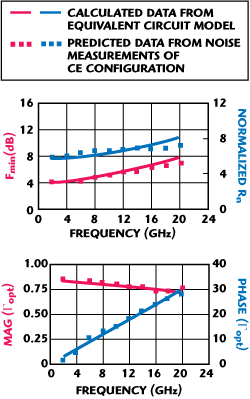
Figure 7 Comparison of modeled and predicted noise parameters for the InP HBT in CC configuration.
In Figures 8 and 9, the calculated noise parameters in the low frequency ranges (Equations 21 to 28) are compared with the predicted data versus frequency for the intrinsic InP HBT device under the same bias condition. Good agreement is obtained between measured and predicted data in the CB and CC configurations, which verifies the proposed approach for the noise parameters.

Figure 8 Comparison of modeled and predicted parameters for the InP HBT in CB configuration at low frequency range.

Figure 9 Comparison of modeled and predicted noise parameters at the low frequency ranges for the InP HBT in CC configuration.
Conclusion
In this article, a set of new analytical expressions for the relationship between common emitter, common base and common collector microwave HBTs is proposed. All the relationships provide a bi-directional bridge for the transformation between CE, CB and CC devices. This technique is based on the combination of an equivalent circuit model and a conventional two-port network signal/noise correlation matrix technique. The validity of the new approach is proved by comparison with measured S- and noise-parameters up to 20 GHz. A good agreement has been obtained for InP/InGaAs DHBTs with a 5 x 5 µm2 emitter area.
Acknowledgment
This work was supported by the National Natural Science Foundation of China under grant No. 60671054 and New Century Excellent Talent from the Ministry of Education in China.
References
1. K.W. Kobayashi and A.K. Oki, “A Low-noise Baseband 5 GHz Direct-coupled HBT Amplifier with Common-base Active Input Match,” IEEE Microwave and Guided Wave Letters, Vol. 4, No. 11, November 1994, pp. 373-375.
2. H. Wang, K.W. Chang, L.T. Tran, J.C. Cowles, T.R. Block, E.W. Lin, G.S. Dow, A.K. Oki, D.C. Streit and B.R. Allen, “Low Phase Noise Millimeter-wave Frequency Sources Using InP-based HBT MMIC Technology,” IEEE Journal of Solid-State Circuits, Vol. 31, No. 10, October 1996, pp. 1419-1425.
3. V.K. Paidi, Z. Griffith, Y. Wei, M. Dahlstrom, M. Urteage, N. Parthasarathy, S. Munkyo, L. Samosha, A. Fung and M.J.W. Rodwell, “G-band (140 to 220 GHz) and W-band (75 to 110 GHz) InP DHBT Medium Power Amplifiers,” IEEE Transactions on Microwave Theory and Techniques, Vol. 53, No. 2, February 2005, pp. 598-605.
4. M. Aiki, “Low-noise Optical Receiver for High-speed Optical Transmission,” IEEE Transactions on Electron Devices, Vol. 32, No. 12, December 1985, pp. 2693-2698.
5. J.S. Lee, J.D. Cressler and A.J. Joseph, “A 5 to 6 GHz SiGe HBT Monolithic Active Isolator for Improving Reverse Isolation in Wireless Systems,” IEEE Microwave and Wireless Components Letters, Vol. 15, No. 4, April 2005, pp. 220-222.
6. H. Hillbrand and P. Russer, “An Efficient Method for Computer-aided Noise Analysis of Linear Amplifier Networks,” IEEE Transactions on Circuits and Systems, Vol. 23, No. 4, April 1976, pp. 235-238.
7. J.B. Hagen, “Noise Parameter Transformations for Three-terminal Amplifiers,” IEEE Transactions on Microwave Theory and Techniques, Vol. 38, No. 3, March 1990, pp. 319-321.
8. J. Gao and G. Boeck, “Relationships Between Common Source, Common Gate and Common Drain FETs,” IEEE Transactions on Microwave Theory and Techniques, Vol. 53, No. 12, December 2005, pp. 3825-3831.
9. J. Gao, X. Li, H. Wang and G. Boeck, “An Approach for Determination of Extrinsic Resistances for Metamorphic InP/InGaAs HBTs Equivalent Circuit Model,” IEEE Proceedings—Microwaves, Antennas and Propagation, Vol. 152, No. 3, 2005, pp. 195-200.
10. J. Gao, X. Li, H. Wang and G. Boeck, “Microwave Noise Modeling for InP/InGaAs HBTs,” IEEE Transactions on Microwave Theory and Techniques, Vol. 52, No. 4, April 2004, pp. 1264-1272.