
Nowadays, microwave antennas are widely used, especially in achieving the objective of maximal integration for personal communication systems. These antennas can be mounted on the surface of high performance aircrafts, satellites, missiles, mobile phones and others. Integrated antennas are a combination of solid-state devices and circuits with printed antenna structures to form integrated radio system elements that are fabricated using inexpensive printed circuit techniques.1 Integrated antennas have become an important area of research because they can give excellent results in term of efficiency, compactness, lightweight and low cost, compared to conventional systems. The main disadvantage of microstrip antennas is an intrinsic limitation in bandwidth, which is due to the resonant nature of the patch structure.2 This problem gives a new motivation in research for solutions to overcome the bandwidth limitations of the microstrip antenna. Applications where an increase in bandwidth for operation at two separate sub-bands are found in dual-frequency microstrip antennas.3,4 This kind of antenna can be more useful for a system that can receive and transmit at the same time.
This article discusses four different architectures of receivers that employ a power dividing patch antenna instead of a discrete power divider, which are applied to an image reject system, a dual-frequency system, a direct conversion receiver and a Butler matrix of smart antennas. These new system design approaches are useful for the RF designer, especially for compact system design requirement.
Integrated Image Reject Mixer (IRM) System
Proposed IRM Receiver Architecture
Different applications for active integrated antenna (AIA) have been rapidly developed, especially for wireless communications.5 The AIA with image rejection, which was developed in this research, introduces a new application of an AIA system.

Figure 1 Conventional approach for image reject system.
A basic and conventional IRM is comprised of a balanced mixer of any topology, driven in quadrature by the radio frequency (RF) signal (see Figure 1). The local oscillator (LO) feeds an in-phase power divider that drives each mixer and the IF output is combined in quadrature.6 The proposed IRM architecture that is developed uses a power dividing patch antenna, as shown in Figure 2. The proposed configuration performs an operation similar to the conventional IRM, but with the phase shifts rearranged. At one of the radiating edges of the patch antenna, a positive maximum signal (+Ve) of a standing wave electric field distribution occurs. The field falls to zero in the center of the patch and a negative maximum (–Ve) occurs at the other radiating edge. Thus, the function f(x) that corresponds to the voltage distribution is odd about the centre of the patch (x=0) such that f(x)=–f(–x). Two microstrip lines are fed along one of the non-radiating edges of the patch, so that the antenna also achieves the function of a 180° hybrid coupler. Therefore, compared to the conventional IRM, the RF hybrid coupler is eliminated or effectively integrated with the operation of the rectangular patch antenna.7 The RF signals are split into two signals, RF1 and RF2, which are 180° out of phase. The 90° difference of the LO signal is mixed to the received RF signals and the IF signals are combined using a 90° hybrid coupler. Therefore, the patch antenna used in the proposed system is closer to the LNA and image reject system and thus should have lower losses compared to the conventional approach.
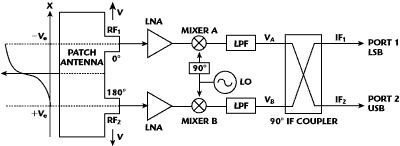
Figure 2 Architecture of proposed image rejection mixer.
IRM Prototype and Measurements

Figure 3 Fabricated layout of the proposed IRM.
The IRM system has been fabricated on two layers of FR4 with εΡ=4.6. The layout is shown in Figure 3. The upper layer is the patch antenna that is connected via through holes to the LNAs and resistive FET mixer system on the bottom layer. The ground plane is the middle layer. The two layers of FR4 are held together by a solder paste placed in the middle and heated so that the ground planes on both layers are joined. The integrated power dividing patch antenna with image rejection has been shown8 to perform an image rejection of approximately 20 dB.

Figure 4 Measured results fo the IRM.
The AIA IRM system was characterized by transmitting a CW RF signal from a separate antenna. The output IF signals from both IF ports are illustrated in the spectrum analyzer printouts in Figure 4, clearly showing the degree of image rejection achieved. The integrated image reject mixer prototype system is shown to perform image rejection with the RF power divider function achieved within the receiving patch antenna. This system can obtain approximately 20 dB image rejection.
Dual-frequency Integrated Antenna (DFIA) with Image Rejection
Proposed DFIA Architecture

Figure 5 Block diagram of the proposed DFIA.
The first active integrated antenna (AIA) with image rejection has been introduced by Maci and Gentili.2 The proposed configuration is similar to theirs, but with the phase shift rearranged and useful for dual-frequency operation. The image reject mixer (IRM) includes two balanced mixers of any topology driven in quadrature by the amplified radio frequency (RF) signal. The LO is applied to an in-phase power divider, which drives each mixer and the IF output power is combined in quadrature. Figure 5 shows the block diagram of the proposed IRM system. In principle, the dual-frequency patch antenna should operate with similar features in terms of both radiation and impedance matching at two separate frequencies. There are many techniques to obtain a dual-frequency patch antenna, such as orthogonal-mode, multi-layer patch and reactively loaded. Maci and Gentili2 introduced many of these techniques and one is used in the present system. A single layer slotted square patch antenna is used to provide the dual-frequency operation. Using two pairs of orthogonal slots, as shown, produces the dual-frequency antenna.
Design Procedure and Testing of DFIA

Figure 6 Patch dimensions (a) and antenna simulation results (b).
A square patch antenna of length and width of 35 mm is designed using FR4 with a dielectric constant of 4.5 and a height of 1.6 mm. The slots’ length is 29 mm and the width is 1 mm. The slots are 1 mm away from the patch edges. The square patch antenna is simulated using Advanced Design System (ADS) Momentum analysis software from Agilent Technologies. The simulation result shows that the square patch antenna designed can perform at dual-band frequencies: at 2.031 GHz with a return loss of approximately 29.28 dB and at 2.408 GHz with a return loss of approximately 23.32 dB, as shown in Figure 6. A MGA-83563 low noise amplifier from Agilent Technologies is used to boost the received signal by approximately 22 dB (from 0.5 to 6 GHz). A balanced resistive FET mixer is designed using Agilent ATF-34143. The mixer operates at 0 V DC bias at the drain and only the gate needs to be biased, while the source is grounded. A 90° hybrid coupler is used to combine the two IF outputs at 70 MHz. The square patch antenna is connected to the LNA and IRM through via holes to complete the circuit of the DFIA with image rejection. The system is simulated using ADS Harmonic Balance circuit simulator.
Simulation and Measurement Results of DFIA
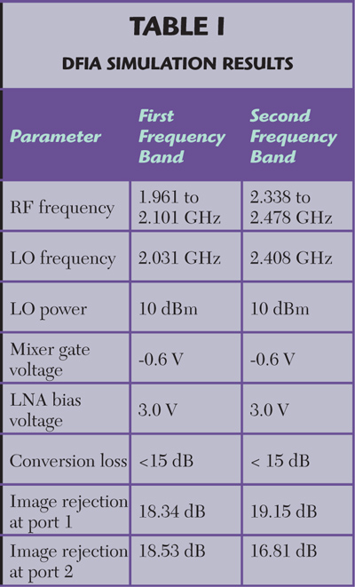
Table 1 DFIA Simulation Test Results
The simulation results show that image rejection is achieved as summarized in Table 1. Image rejection results for both frequencies are acceptable. The prototype of the DFIA image reject system was fabricated on two layers of FR4. Figures 7 and 8 show the layout of the system. The upper layer is the dual-frequency patch antenna, whereas the LNAs and the resistive FET mixer system are on the bottom layer. The two layers are connected via through holes.

Figure 7 Upper layer of the fabricated DFIA (patch antenna).

Figure 8 Bottom layer of the DFIA (image reject system).
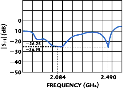
Figure 9 Return loss of the dual-frequency square patch antenna.
The measured return loss of the dual-frequency patch antenna is shown in Figure 9. Clearly, it has shown that the dual-frequency with acceptable return loss is achieved. The first resonant frequency is at 2.084 GHz with return loss around 26.25 dB, which can support the UMTS or CDMA wireless standards. The second frequency is at 2.49 GHz with a return loss of about 26.95 dB that can support Bluetooth, Wi-Fi or WiMAX wireless standards.
Two signal generators were used for transmitting the RF and LO signals. The signal generator for the LO is connected using an in-phase power divider to produce two LO signals that will be applied as the input to two mixers. Four power supplies were used to bias the two LNAs and two mixers. The measurement started by setting the LO frequency at 2.084 GHz and transmit the RF signal at 2.014 GHz using a dipole antenna. The output at port 1 from the external 90° IF power combiner is terminated in 50 Ω to obtain the wanted IF signal at the output in port 2 for LSB. The same method is used for the USB by transmitting the RF signal at 2.154 GHz and terminating port 2 with 50 Ω to obtain the wanted IF signal at port 1.
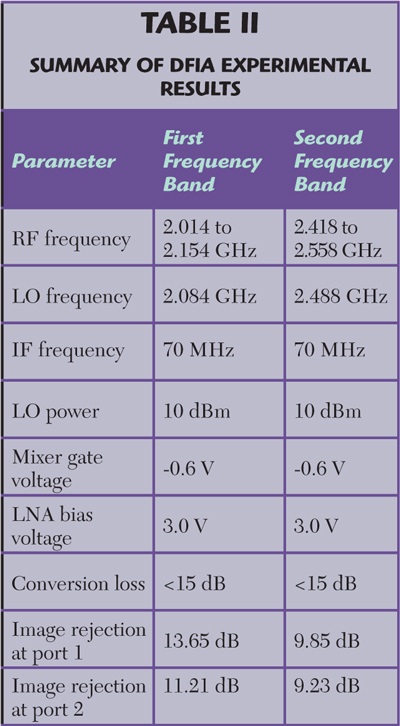
Table 2 Summary of DFIA Experimental Results
Similarly, the same method is used by setting the LO frequency at 2.488 GHz and transmit the RF signal at 2.418 GHz; the wanted signal appears at port 1 for LSB. Then the RF signal at 2.558 GHz is transmitted to obtain the wanted signal at port 2 for USB. The system experimental setup and measurement results for the open-air measurement are summarized in Table 2. Clearly, it shows that the image rejection of approximately 10 dB has been produced, slightly less compared to the simulation results, due to open-air measurements.
It has been shown that the fabricated square patch antenna image reject system can reject the images to two different ports for two different operating frequencies using the same antenna. Phase cancellations are performed with image rejection of approximately 10 dB. Therefore, this architecture introduces a new technique in up-/down-conversion and modulation; thus, it is suitable as a transmitter and receiver at the same time that can support more than one wireless standard through the use of the dual-frequency operations.
Integrated Direct Conversion Receiver (DCR) System
Proposed DCR Receiver Architecture

Figure 10 Proposed architecture of DCR.
A new configuration of direct conversion receiver with integrated power dividing patch antenna is developed for wireless application. The schematic of the proposed DCR with AIA system for WCDMA applications is shown in Figure 10. In this receiver design, dual feed microstrip lines of a power dividing patch antenna are used to provide the odd-mode propagating characteristic that acts as a 180° hybrid coupler which is used in the conventional design. This eliminates the necessity of using an RF hybrid coupler to split the RF power and obtain the proper 180° phase shift difference into DCR system. Two low-noise amplifiers (LNA) are employed to improve the noise performance of the radio frequency (RF) signal, which are out-of-phase to each other. The local oscillator (LO) signal is applied to the gates of each mixer, with a 90° phase shift. The baseband signals are extracted from the drain of each mixer. The desired signals of I and Q components at the baseband frequency are extracted and then filtered using a low pass filter (LPF).
Design Procedure and Testing of the Proposed DCR
Power Dividing Antenna:
The concept of integrating a power-combining patch antenna has been described previously.9,10 It is based on using the dual feeds to excite the proper mode profile in the antenna at the fundamental frequency and suppressing the radiation mode for the higher harmonics. A similar idea is applied in this proposed design in which a power dividing antenna is integrated, based on using a dual feed at one of the non-radiating edges of the patch antenna. This removes the necessity for a 180° RF power splitter. In the 3G WCDMA system, the RF receiving frequency band is from 2110 to 2170 MHz. Thus, the LO frequency is set to be at the center of the system bandwidth, which is 2140 MHz. The power dividing antenna layout, which was fabricated on a Duroid (εΡ=5.4) substrate, is shown in Figure 11.

Figure 11 Power dividing patch antenna prototype.
The two-port network of the patch antenna is decomposed into odd- and even-mode excitation. The patch antenna should work in the odd-mode in order to provide the power dividing function. The S11odd (S11–S12) and S22odd (S22–S21) in dB are defined as the ratio of the odd-reflected voltage to the odd-incident voltage wave at port 1 and port 2, respectively. The S11even (S11+ S12) and S22even (S22+ S21) in dB are characterized for the even-mode excitation for port 1 and port 2, respectively. The S-parameter’s measurement is carried out using a network analyzer. The odd-mode and even-mode excitation results are shown in Figure 12. The measured results of the odd-mode excitation (S11odd and S22odd) show that a return loss of –12.111 dB and –11.063 dB at the center frequency of 2.39 GHz, respectively, where the offset frequency is 0.25 GHz.

Figure 12 Odd- and even-mode excitation measurement results.

Figure 13 DCR circuit prototype.
DCR System:
Figure 13 shows the fabricated prototype of the DCR system. The mixers in the DCR design are implemented using a FET resistive mixer and a single balanced mixer topology. The advantages of the FET balanced mixer are low levels of intermodulation distortion and spurious responses and high 1 dB compression point.11 The ATF 34143 PHEMT mixer from Agilent is employed because it offers better conversion loss than MESFETs. In addition, it has low noise figure (0.5 dB), high 1 dB gain compression (20 dBm) and a high third-order intercept point (IIP3) of 31.5 dBm. The LO signal is divided into two 90° phase difference signals using a Mini-Circuits QBA-24W splitter. The low pass filter is formed by LC-lumped element component to extract the I and Q signals.

Figure 14 Measured I and Q signals from an oscilloscope.
System Measurements:
The RF signal of 2.15 GHz and the LO signal of 2.14 GHz are applied to the DCR system, so that the IF frequency is obtained at 10 MHz. The measured offset IF is 1.15 MHz. Figure 14 shows that the I and Q components with 90° phase difference characteristics are achieved for the direct conversion purposes. This new direct conversion with active integrated antenna has been presented. The integrated power dividing antenna with DCR architecture yields a compact front-end receiver. The measurement results of the I and Q signals demonstrated that the down-converted QPSK signal has been successfully achieved.
4 x 4 Butler Matrix of Smart Antenna
Proposed Smart Antenna
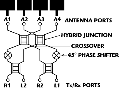
Figure 15 Conventional 4 x 4 Butler matrix.
Smart antennas have recently received increasing interest for improving wireless systems.12 The so-called 4 x 4 Butler matrix is a passive circuit, which gives the ability to get a main beam from an antenna array into one of the four beam directions, as shown in Figure 15. The matrix is designed at 2 GHz and implemented on a microstrip structure using conventional manufacturing processes. The matrix consists of hybrid couplers, a crossover, phase shifters and power dividing patch antennas. The main purpose of this research is to reduce the number of couplers and antennas in the matrix from the original design. The matrix is designed and simulated, using ADS. The measurements that are of concern in this project are return losses, phase shifts, antenna gain and radiation patterns. The new design’s results will be compared with the original and may prove that the new design operates in the same way. The new design’s patch antenna shows a 180° phase shift at the edges. It may replace the hybrid couplers function in the original design’s Butler matrix and the number of couplers may be reduced from four to two. Since there are two ports at each patch antenna, the number of antennas may be reduced from four to two also. The simulation results of the new design are being compared with the original design to prove the new design is workable. The physical implementation of the matrix consists of four hybrid couplers, two crossovers and two 45° phase shifters.13 The matrix had been designed and simulated using ADS. The return loss and phase shift of each output were considered. However, the design was optimized to obtain better results. Figure 16 shows the proposed block diagram of a 4 x 4 Butler matrix. By comparing with theoretical phase shift14 (see Table 3), the simulation results are similar with only 15 percent phase difference, as shown in Table 4.

Figure 16 Proposed 4 x 4 Butler matrix using power dividing patch antenna.

Table 3 Theoretical Input-Output Phase Shift of a 4 x 4 Butler Matrix

Table 4 Input-Output Phase Difference of the Proposed Design

Figure 17 Radiation pattern of the power dividing patch antenna.
The radiation pattern of the antenna used for the proposed integrated 4 x 4 Butler matrix is shown in Figure 17. The radiation pattern is similar to the simulation results and is acceptable. The maximum pattern received by the patch antenna occurs when the transmitter and receiver are facing directly at 90°. Then a minimum happens when the antenna faces 270° from the dipole because the antenna ground plane prevents any signal from the transmitter to be received. The radiation pattern for the fabricated integrated Butler matrix is shown in Figure 18. It shows that the pattern is similar for port 1 and port 4 when they are fed or when port 2 and port 3 are fed. From the pattern, it can be seen that there are four beams occur in the pattern. This is important evidence showing that the new design antenna is operating in a way similar to the original Butler matrix.

Figure 18 Radiation patterns of the integrated Butler matrix.
The objective of this project was to reduce the number of couplers and patch antennas. This has been proven by comparing the new design results with the original Butler matrix’s results. This project has shown that it is possible to reduce the number of hybrid couplers and patch antennas in a 4 x 4 Butler matrix. The measured radiation patterns of the new design show that it is operating in a way similar to the original Butler matrix.
Conclusion
Four designs of integrated power dividing patch antennas have been discussed. The first architecture has shown to perform image rejection of approximately 20 dB, while the second one is similar but with the application for dual-band frequency. The third architecture has been shown to perform direct conversion with I and Q modulation. The fourth architecture is for a smart antenna system, using a 4 x 4 Butler matrix that reduces the number of antennas used from four to two, while maintaining the same performance. Therefore, all these four architectures eliminate the use of power dividers since their function is achieved by the antenna itself.
Four new approaches in front-end receiver design are presented. These four designs have shown to be compact and produced similar performance to the conventional design. Therefore, this system is useful for system designers if space is critical (in IC design, for example). It can also be used for other receiver applications by employing the power dividing antenna at the front-end.
Acknowledgment
The authors wish to acknowledge the support and contributions of all those who assisted in this research, and especially Universiti Sains Malaysia for sponsoring it.
References
1. W.P. Carl and T. Itoh, “Active Integrated Antennas,” IEEE Potentials 1997.
2. S. Maci and B. Gentili, “Dual-frequency Patch Antenna,” IEEE Antennas and Propagation Magazine, Vol. 39, No. 6, December 1997, pp. 13-20.
3. H.W. Tseng, R. Kurtz, A. Brown, D. Nathans and F. Pahr, “Test Results of a Dual-frequency (L1/L2) Small Controlled Reception Pattern Antenna,” Proceedings of ION NTM 2002, San Diego, CA.
4. J.Y. Jan, “Single-layer Single-feed Dual-frequency Circular Microstrip Antenna with an Offset Open-ring Slot,” IEEE Transactions on Antennas and Propagation, Vol. 51, No. 10, Part 2, October 2003, pp. 3010-3012.
5. K. Chang, R.A. York, P.S. Hall and T. Itoh, “Active Integrated Antennas,” IEEE Transactions on Microwave Theory and Techniques, Vol. 50, No. 3, March 2002, pp. 937-944.
6. B.C. Handerson and J.A. Cook, “Image-reject and Single-sideband Mixers,” Technical Note from WJ Communication Inc. (2002), available at www.wj.com.
7. S. Anuar, Z, Murad and W. Ismail, “Design of Active Integrated Antenna for Dual-frequency Image Rejection,” American Journal of Applied Sciences, Vol. 3, No. 6, 2006 Science Publication, pp. 1890-1894.
8. W. Ismail and P. Gardner, “Active Integrated Antenna with Image Rejection,” International European Microwave Conference on Wireless Technology Digest, Munich, Germany, September 2003.
9. S.T. Chiw, P. Gardner and S.C. Gao, “Compact Power Combining Patch Antenna,” Electronics Letters, Vol. 38, No. 23, 2002, pp. 1413-1414.
10. W.R. Deal, V. Radisic, Y. Qian and T. Itoh, “Novel Push-pull Integrated Antenna Transmitter Front-end,” IEEE Microwave and Guided Wave Letters, Vol. 8, No. 11, November 1998, pp. 405-407.
11. S.A. Maas, “A GaAs MESFET Mixer with Very Low Intermodulation,” IEEE Transactions on Microwave Theory and Techniques, Vol. 35, No. 4, April 1987, pp. 425-429.
12. M. Chryssomallis, “Smart Antennas,” IEEE Antennas and Propagation Magazine, Vol. 42, No. 3, June 2000, pp. 129-136.
13. S.I. Yamamoto, J. Hirokawa and M. Ando, “A Half-sized Post Wall Short Slot Directional Coupler with Hollow Rectangular Holes in a Dielectric Substrate,” IEICE Transaction on Electronics, Vol. E88-C, No. 7, July 2005, pp. 1387-394.
14. S.C. Gao, L.W. Li, M.S. Leong and T.S. Yeo, “Integrated Multibeam Dual-polarized Planar Array,” IEEE Proceedings on Microwave and Antenna Propagation, Vol. 148, No. 3, June 2001, pp. 174-178.