
 The recent launch of Freescale RF high power, high voltage LDMOS devices has made possible the design of kilowatt class power amplifiers in a compact format. A 1 kW power amplifier operating in pulse mode at 27.5 MHz intended for ISM applications has been designed. It is targeted for high power applications using a single push-pull device in a symmetric configuration for use in MRI as a RF source building block for multi-kilowatt power amplifiers. The MRF6VP11KH is a 50 V LDMOS device capable of exceeding 1000 W RF pulse output power at 130 MHz at a large-signal gain of 26 dB in Class AB2 and a drain efficiency of 71 percent. It can handle 10:1 VSWR at Vds of 50 VDC, 130 MHz at 1000 W peak power. The ceramic package is a NI-1230 size, case 375D-05, style 1 with gold plated flanges.
Component Selection
At high power levels, large DC and RF currents flow through the circuit and components. Hence, it is important to design and dimension the PC board traces, capacitors, inductors and transformers to operate safely at the rated output RF power of 1 kW. Component selection pointed to the following:
- Gate DC bias decoupling network: a four-stage circuit to reduce power supply noise and provide RF bypass. The first stage is comprised of electrolytic and tantalum bypass capacitors with low ESR to locally reduce ripple and noise, followed by a two-stage LC network that provides RF decoupling via ceramic capacitors. A final RC stage ensures RF bypass before entering the input coupling transformer. The multi-stage approach assures stable operation as the amplifier operates at high gain.
- Input RF sub-network: ceramic capacitors and ferrite core input matching transformer to reduce leakage inductance and improve coupling between primary and secondary.
- Drain DC bias decoupling network: a three-stage circuit to reduce power supply noise and provide RF return to ground. The first stage has electrolytic bypass capacitors with low ESR to locally reduce ripple and noise, followed by a two-stage LC network that provides RF decoupling via ceramic capacitors. Additional RF return to ground is provided by two low ESR ceramic capacitors in parallel at the output transformer primary center-tap. The DC power supply Vsense line has a separate connection to minimize voltage drop in the circuit.
- Output RF sub-network: mica HV capacitors and large ferrite core output matching transformer able to carry the maximum power with low loss.
Final component values are given in Table 1.
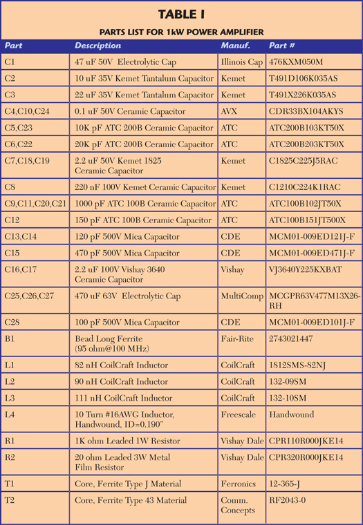
Table 1 Parts List for 1kW Power Amplifier
With an estimated drain efficiency of 65 percent, this represents a heat generation of 35 percent of the DC input power. The thermal design is an important consideration for high power amplifiers as the junction temperature (Tj) must be kept below 200°C, otherwise the device reliability in terms of MTTF will be impacted. A 5 by 5 inch pin fin type heat sink with a Cu heat spreader was selected. Forced air through the fin pins is used to remove the heat generated during test. In order to minimize the source contact thermal impedance, a small amount of thermal grease compound is applied to the source flange to create a thin layer (1 mil).
PC Board Layout and Parts List
In general, the LDMOS RF power devices present a low input and output impedance. Thus, input and output matching transformers are required. An associated insertion loss at the input and output can be estimated due to a non-unity coupling factor, leakage inductance and core losses. However, these can be minimized by the use of ferrite cores in both cases. A binocular type ferrite core is used for the input and a commercially available blank core transformer with sleeve ferrites for the output. It was determined that a 2:1 turns ratio (4:1 impedance ratio) input transformer was satisfactory and a 1:3 turns ratio (1:9 impedance ratio) for the output was near optimum.

Figure 1 Parts assembly and PC board layout.
The parts assembly diagram and printed circuit board layout are shown in Figure 1 (the parts list is given in Table 1). No mechanical hardware is mentioned, as it depends on the final packaging solution chosen. The circuit diagram is shown in Figure 2 and a picture of the assembled board without the output transformer is shown in Figure 3. A top view of the finalized board is shown in Figure 4. Designators and values can be found in the parts list.
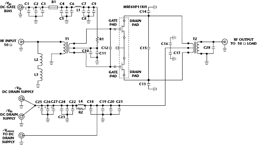
Figure 2 Circuit diagram.

Figure 3 Photo of assembled board without output transformer.

Figure 4 Complete assembled board.
Ferrite core transformers are used in this application for higher efficiency and compact form factor. Input transformer T1 is wound 2:1 turns ratio (4:1 impedance ratio) on a binocular type core. Primary is 2 turns No. 22 AWG plastic insulated stranded copper wire and secondary is 1 turn with centre tap No. 22 AWG Teflon insulated wire. Primary is wound first tight against the core, followed by the secondary. Different wire colors can easily identify the windings. Output transformer T2 is wound 3:1 turns ratio (1:9 impedance ratio) on a ferrite core which already has a 1 turn copper tube primary with CT. Secondary is 3 turns No. 16 AWG Teflon insulated stranded copper wire. Secondary is wound tight against the core to minimize leakage inductance.
Performance
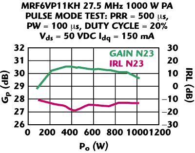
Figure 5 Large signal gain and input return loss vs. output power.
Measured performance of the power amplifier test fixture is given in Figure 5 as a graph of large signal gain Gp versus output RF power Po. In the same figure, the input return loss IRL is plotted against Po. Gain compression at Po, slightly above 1 kW, is ΔGp≤1 dB. Figure 6 shows a graph of drain efficiency versus Po and drain current Ids with Vds at 50 VDC and Idq at 150 mA. The maximum efficiency is 58 percent at 1 kW of output power.

Figure 6 Drain efficiency vs. output power and current.
Conclusion
A test circuit using a high power LDMOS transistor operating at 27.5 MHz and capable of delivering 1000 W pulse power into the load demonstrates the application of the Freescale MRF6VP11KH. The test fixture exhibits high gain and reasonably good efficiency at maximum power in pulse mode with PRR=500 μs, PW=100 μs and duty cycle=20 percent. The second harmonic measured level is -45 dBc, which is a good indication of the input and output network balance. The third harmonic level is -27 dBc typical at Po 1000 W.
Freescale Semiconductor,
Austin, TX (800) 521-6274, www.freescale.com.
RS No. 301