
The high power and wide bandwidth potential of GaN HEMT devices is well known.1 RFMD has been developing high power amplifiers using GaN HEMTs for various applications. A 250 W amplifier in the 2.14 to 2.5 GHz band for wireless infrastructure applications in the WCDMA and WiMAX bands was reported previously.2 Such wide bandwidth is essential for the next-generation frequency agile software-defined radio (SDR) architectures that use reconfigurable radios to support multiple frequency bands and various standards.3
The military and commercial communities require high power and broadband modules for pulsed radar surveillance and air traffic control applications. The market is looking for the next-generation of devices that provide higher power and broader bandwidth and are able to support 1.2 to 1.4 GHz L-band for IFF, TACAN and TCAS pulsed applications and 2.7 to 3.5 GHz S-band pulsed applications. These devices will enable suppliers to power combine fewer devices and reduce the size and weight power modules of greater than 1 kW for use in radar systems.
To obtain high power in existing power amplifier technologies, such as silicon laterally diffused metal oxide semiconductor (Si LDMOS) and gallium arsenide pseudomorphic high electron mobility (GaAs PHEMT), large periphery devices are required. The resulting inherent large device parasitic capacitances per watt of output power lead to low device input and output impedances. Matching such low impedance to a 50 Ω system severely limits the bandwidth achievable. This also limits the maximum power obtainable in a package and further power combining is needed on the board. Wide band-gap material systems like gallium nitride (GaN) can be operated at high drain voltage and have low parasitic capacitances per watt of output power. A combination of wider bandwidth and high output power can be achieved in a small package. This simplifies the design of kW transmitters for radar and jamming applications by reducing the number of devices required and minimizing losses in external combining networks.
Theory
In theory, purely real impedances can be matched to a 50 Ω system over any bandwidth using an infinite number of matching elements. However, actual devices have optimum impedances with a reactive component. Complex loads can be matched only over a limited bandwidth as defined by Fano’s limit.4 The maximum bandwidth ratio achieved using an infinite lossless matching network is given by
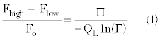
where QL is the Q-factor of the device optimum source or load impedance to be matched and Γ is the minimum reflection coefficient needed across the band. This bandwidth is further limited in practice due to the finite number of matching sections and the matching network losses. Hence, low Q-factors for the optimum source and load impedances are critical to obtaining a broad bandwidth. A suitable figure of merit, for high power broadband capability of a device technology, is a low pF/W gate and drain capacitance.
GaN HEMT Technology
RFMD’s baseline AlGaN/GaN HEMT technology is based on devices with a standard 0.5 μm gate length and an advanced source connected field plate to obtain breakdown voltages in excess of 150 V. To be able to handle high-power densities in excess of 10 W/mm, a SiC substrate is used that provides excellent thermal conductivity and minimizes temperature dependent memory effects. The device topology and the baseline fabrication process are detailed in an earlier publication.5

Table 1 Summary of GaN Process DC Parameters

Figure 1 GaN unit cell current and power gain performance.
Typical dc characteristics for the gallium nitride HEMT process are provided in Table 1. A typical device, biased at a drain voltage of 65 V, exhibits a peak current density of 0.9 A/mm. The current and power gain cut-off frequencies (ft and fmax), as measured from small periphery devices, are 11 and 18 GHz respectively, as shown in Figure 1.
Under class AB bias and CW operation at 3.3 GHz, a typical 2.2 mm unit cell device obtains 56 percent peak power added efficiency (PAE) and a peak output power of 21.9 W. This corresponds to a power density of 9.9 W/mm. This is about three times the 3.2 W/mm power density obtained at 28 V drain bias from a device without the field plate. The series equivalent optimum source and load impedances are Zs= 3.8 + j10.5 Ω and Zl=30 + j47 Ω, respectively. These indicate low gate and drain capacitances of approximately 0.46 pF/W and 0.07 pF/W, respectively, which is about one fifth of that of equivalent silicon devices. Using this series equivalent source impedance, the theoretical maximum bandwidth ratio for a 15 dB return loss can be calculated to be 57 percent. These low capacitances contribute to the higher bandwidth obtained, compared to other device technologies.
Circuit Design
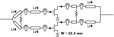
Figure 2 Schematic of the amplifier circuit.
The amplifier circuit, seen in Figure 2, uses two 22.2 mm periphery devices, combined using a Wilkinson power divider/combiner6 on the input and output, respectively. This topology achieves a wider bandwidth than would be obtained using a single 44.4 mm device. Along with the power division/combination function, the Wilkinson combiners also perform the impedance transformations required to provide the optimum source and load impedance to the devices.
The unit cell source and load pull impedance measurements were used to estimate the large periphery device’s source and load optimum impedances. Due to the higher gate capacitance, a two-stage impedance transformation was used at the gate to obtain a broader bandwidth. The drain section consists of an inductive element to provide the reactance needed for the optimum load and a single stage Wilkinson combiner/transformer. Electromagnetic field models were used extensively to model the frequency performance of the combiner transformer elements.
Additionally, extensive stability analysis and odd-mode oscillation loop analysis were conducted. This type of combining network is prone to the formation of out of frequency band oscillation loops. Therefore, the design needs significant analysis over a wide frequency range to determine if any potential odd-mode oscillation loops exist. A previous work7 provides a detailed description of applying stability analysis to multi-device amplifiers, using linear analysis and S-parameters. Applying this methodology to gallium-nitride-based amplifiers, an extensive analysis of odd-mode oscillation loops is provided by Yanamaka, et al.8 For an odd-mode loop to cause stability issues, the following conditions must be met
Loop phase angle (Γ)=0° (2)
Loop gain magnitude (Γ)>1 (0 dB) (3)
Generally, however, to provide adequate design margin, loop gain less than -2 dB should be maintained across a frequency band where Gmax is greater than 0 dB.
A similar methodology was applied to this amplifier design; an example of the loop analysis is shown in Figure 3. The amplifier’s loop gain and phase, using Wilkinson combiner networks not using an isolation resistor between the ports, is shown. It can be seen that the loop phase angle meets the criteria for oscillation at two distinct frequencies 3.685 and 8.536 GHz. Additionally, the loop phase is close to the criterion at low frequency. In all three cases the loop gain requirement is not met. However, the loop gain margin is less than the adequate limit defined. The figure also shows how the loop stability can be increased by adding an isolation resistor to the Wilkinson combiner and by optimizing the gallium nitride device layout. The loop gain has been reduced to levels meeting the design margin requirements at all three frequency points.

Figure 4 Photograph of the 400 W GaN HEMT amplifier.

Figure 5 Photograph of the 400 W 50 Ω test fixture.
The devices are packaged in a 15 x 17 mm package (see Figure 4).9 The combiner/dividers were implemented on high dielectric constant substrates to achieve the small dimensions required to fit inside the package. The quarter-wave transformations were designed to obtain a 35 Ω impedance at the package leads. The evaluation board used for testing further transforms the impedance to 50 W and is shown in Figure 5.
Pulse Power Performance
The RF performance of the device was evaluated after optimizing the on-board matching. The amplifier was biased in class AB mode at a fixed drain voltage of 65 V and a drain current of 440 mA. The RF input was pulsed using a 100 μs wide pulse with a 1 ms period and the output power was measured at the center of the pulse. The drain current pulse waveform was monitored to calculate the drain efficiency. The amplifier was tested over the frequency range of 2.9 to 3.5 GHz.

Figure 6 RF output power at the mid-point of the pulse, drain efficiency and gain measured at 3.4 GHz.

Figure 7 RF output power at the mid-point of the pulse over the 2.9 to 3.5 GHz band.
Figure 6 shows the measured output power at the mid-point of the pulse, the drain efficiency and the gain at 3.4 GHz as a function of the input power. A peak output power of 434 W was obtained at 3.4 GHz with a drain efficiency of 52.6 percent. Figure 7 shows the measured output power over frequency for a range of input power. The broadband power capability of the device is apparent from the plot.

Figure 8 Measured saturated output power and drain efficiency over the 2.9 to 3.5 GHz frequency band.

Table 2 Summary of the Amplifier RF Performance
Figure 8 shows the peak saturated output power and drain efficiency over the frequency band, while Table 2 summarizes the data. An output power in excess of 401.5 W was obtained over the entire band, with better than 48.4 percent drain efficiency.

Figure 9 Measured power droop of 0.25 dB over a 100 μs pulse at 56.4 dBm output power (at the center of the pulse) with 10% duty cycle.
The pulse droop performance at 56.4 dBm output power (see Figure 9) shows approximately a 0.25 dB droop over the complete 100 μs pulse, and less than 0.15 dB across the middle 50 percent of the pulse. This confirms the excellent thermal capability of the GaN on SiC dies in the package, even under the high power density at which they are operating.
Conclusion
A compact, greater than 400 W, wideband, AlGaN/GaN HEMT power amplifier has been demonstrated, operating at 65 V with better than 48.4 percent drain efficiency over a 600 MHz bandwidth from 2.9 to 3.5 GHz, under pulsed condition with a 10 percent duty cycle and 100 μs pulse width.
The combination of GaN HEMT device technology and the impedance matching topology achieves high power and broad bandwidth in a small package. The design incorporates Wilkinson combiner/transformers that provide excellent low loss, wide bandwidth performance in a compact design. The loop stability is a critical design consideration that was addressed to ensure stability over all frequencies.
These amplifiers are well suited for pulsed applications, including advanced radar systems. The small size and high power obtained in a single package greatly simplifies the design of kW transmitters by reducing the number of devices needed in parallel. In addition, improvement to overall system bandwidth and efficiency is achieved as the combiner losses are further reduced. Additional savings in inventory and critical real estate needs are further advantages of using this device.
Acknowledgment
The authors wish to acknowledge their colleagues at RFMD for their continued and timely support in device fabrication and assembly.
References
1. L.F. Eastman, et al., “The Toughest Transistor Yet [GaN Transistors],” IEEE Spectrum, Vol. 39, No. 5, May 2002.
2. K. Krishnamurthy, M.J. Poulton, J. Martin, R. Vetury, J.D. Brown and J.B. Shealy, “A 250 W S-band GaN HEMT Amplifier,” 2007 IEEE Compound Semiconductor Integrated Circuit Symposium Digest, pp. 1-4.
3. W. Koenig, S. Walter, U. Weiss and D. Wiegner, “A Multi-band Front-end for a Medium Range Base Station: An Important Step Towards SDR,” Third Karlsruhe Workshop on Software Radios, WSR’04, March 17-18, 2004.
4. R.M. Fano, “Theoretical Limitations on the Broadband Matching of Arbitrary Impedances,” Journal of the Franklin Institute, January 1950.
5. R. Vetury, Y. Wei, D.S. Green, S.R. Gibb, T.W. Mercier, K. Leverich, P.M. Garber, M.J. Poulton and J.B. Shealy, “High Power, High Efficiency, AlGaN/GaN HEMT Technology for Wireless Base Station Applications,” 2005 IEEE MTT-S International Microwave Symposium Digest, June 2005, pp. 487-490.
6. E. Wilkinson, “An N-way Hybrid Power Divider,” IRE Transactions on Microwave Theory and Techniques, Vol. 8, No. 1, January 1960, pp. 116-118.
7. M. Ohtomo, “Stability Analysis and Numerical Simulation of Multidevice Amplifiers,” IEEE Transactions on Microwave Theory and Techniques, Vol. 41, No. 6/7, June/July 1993, pp. 983-991.
8. K. Yamanaka, K. Iyomasa, H. Ohtsuka, M. Nakayama, Y. Tsuyama, T. Kunii, Y. Kamo and T. Takagi, “S- and C-band Over 100 W GaN HEMT 1 Chip High Power Amplifiers with Cell Division Configuration,” 2005 European Gallium Arsenide and Other Semiconductor Application Symposium Digest, pp. 241-244.
9. K. Krishnamurthy, J. Martin, B. Landberg, R. Vetury and M.J. Poulton, “Wideband 400 W Pulsed Power GaN HEMT Amplifiers,” 2008 IEEE MTT-S International Microwave Symposium Digest, June 2008, pp. 303-306.
Matthew Poulton received a BSc in Physics from University of Birmingham, Birmingham, UK, an MSc in Microwave Solid State Physics from University of Portsmouth, Portsmouth, UK and has 14 years of experience in microwave product and IC development, and engineering management. He is currently a principal engineer at RFMD’s Aerospace and Defense business unit, based in Charlotte, North Carolina. For the last seven years Mr. Poulton has contributed to GaN HEMT device development and high power amplifier design using RFMD’s gallium nitride HEMT technology.
Karthik Krishnamurthy received the B.Tech. degree from the Indian Institute of Technology, Chennai, in 1995, and the M.S. and Ph.D. degrees from the University of California, Santa Barbara (UCSB), in 1996 and 2000, respectively. He is currently a staff design engineer at the Aerospace and Defense business unit of RF Micro Devices, Charlotte Design Center. His current work focuses on circuits and devices for high power and ultra-broadband efficient RF/microwave power amplifiers in AlGaN/GaN HEMT technology.
James Martin received a Bachelor of Engineering in Electrical Engineering from Vanderbilt University in Nashville, TN and has 13 years of experience in the design of RF and MW integrated circuits and engineering management. He is currently an Engineering Manager within RFMD’s Aerospace and Defense business unit, based in Charlotte, North Carolina. Current areas of focus include GaN and GaAs based products for military communications, Radar, jamming, and other general purpose amplifier applications in the defense sphere.
Bart Landberg is a product engineer who specializes in test and measurement automation at RFMD. He holds a BSEET from UNC-Charlotte.
Ramakrishna Vetury received his B.Tech degree from the Indian Institute of Technology, Madras and his MSEE and PhD degrees from the University of California at Santa Barbara. He has published in the areas of solid state devices and circuits and is currently working in the development of gallium nitride based FET technologies at RFMD.
David Aichele is Director, Business Development with the Aerospace & Defense Business Group of RFMD. David has been with RFMD for the past 4 years and prior to that held strategic positions with Tessera Technologies (formerly Digital Optics) and Tyco Electronics. David holds a MBA focus on Technology Innovation from University of Colorado and a BSEE from Ohio University.