
A simple method for the extraction of the small-signal model parameters of a MOSFET is proposed. The intrinsic elements determined are described as functions of the extrinsic resistances. The parasitic elements are iteratively determined using the variance of the intrinsic elements as an optimization criterion. Good agreement is obtained between simulated and measured results over a wide range of bias points up to 30 GHz.
For the fabrication of high-performance CMOS RF/microwave IC modules, suitable IC design and device characterization technologies for high-frequency applications should be well established. A critical issue in the technologies is the development of a physically acceptable small-signal MOSFET model and an accurate parameter extraction technique, which are crucial to design linear RF ICs such as low noise amplifiers and develop a large-signal model for nonlinear RF IC design. In addition, this small-signal modeling is increasingly important because the device characteristic data used for optimizing RF device performance during the development cycle of process integration can be provided through the extraction of small-signal model parameters.1
An accurate procedure for extraction of the extrinsic resistances is extremely important for silicon MOSFETs. Optimization methods have conventionally been used for the determination of these parameters. However, the accuracy of the numerical optimization methods that minimizes the difference between measured and modeled S-parameters versus frequency can vary, depending upon the optimization method and starting values, and may result in nonphysical and no unique results for the extracted elements.2 For the direct extraction of small-signal MESFET equivalent circuits from S-parameters, parasitic inductances and resistances are initially determined and subsequently the rest of the parameters are extracted from formulations.3,4 However, this cold-FET method cannot be applied to extract these resistances for Si MOSFETs because the DC gate current cannot flow due to the isolation between the gate and the rest of device. As a modified approach5 for Si MOSFETs, extrinsic resistances have been extracted from S-parameters at zero bias condition (VGS = VDS = 0). This method may produce uncertainties due to possible bias dependences in the extraction of source and drain resistances.6 Because of these difficulties, the values of the extrinsic resistances are often guessed or set to zero.7
In this article, an improved method to determine a MOSFET equivalent circuit, including the substrate-related parameters, is proposed. This method combines the advantages of the analytical and optimization extraction methods, and extracted results that are more accurate can be obtained. The intrinsic elements determined are expressed as functions of the extrinsic resistances. Assuming that the equivalent circuit is valid over the whole frequency range of the measurement, the parasitic elements are iteratively determined using the variance of the intrinsic elements as an optimization criterion.
Analytical Determination of the Equivalent Circuit
Parameters Extraction

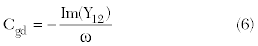
Figure 1 Equivalent circuit of a MOSFET.
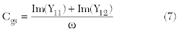
Figure 1 shows the equivalent circuit of a short-channel MOSFET, whose intrinsic behavior is properly modeled by means of a quasi-static (QS) approach. Once the extrinsic resistances are determined, the intrinsic elements can be determined after de-embedding the open and short structures by using four steps as follows:
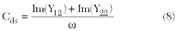
1) Subtraction of Rg and Rd:
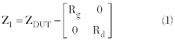
Where ZDUT is the matrix obtained from conversion of the de-embedded S-parameters to the corresponding Z-parameters.
2) Subtraction of the substrate parasitics:
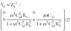
For the case of the substrate elements (Rsub and Csub), the extraction is also biased on the MOSFET’s equivalent circuit model at Vds = Vgs = 0.8 The real part of 1/Z22 at Vds = Vgs = 0 is given by
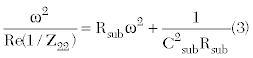
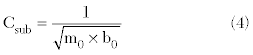
Rsub can be determined from the slope m0 of the linear regression of the ω2/Re(1/Z22) versus ω2 data, whereas Csub is determined from the intercept with the abscissa b0 by applying:
3) Subtraction of Rs:
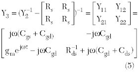
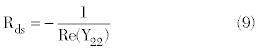
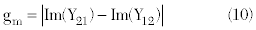
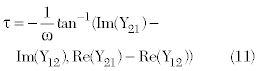
4) Intrinsic Elements
The intrinsic elements can be obtained from the intrinsic Y-parameters.
Criterion of Circuit Validity
The intrinsic elements can be determined by solving Equations 6 to 11 as functions of the extrinsic elements as well as frequency:
Rsub = f0(ωi, Rg, Rd, Rs) (12)
Csub = f1(ωi, Rg, Rd, Rs) (13)
Cgd = f2(ωi, Rg, Rd, Rs) (14)
Cgs = f3(ωi, Rg, Rd, Rs) (15)
Cds = f4 (ωi, Rg, Rd, Rs) (16)
Rds = f5 (ωi, Rg, Rd, Rs) (17)
gm = f6 (ωi, Rg, Rd, Rs) (18)
τm = f7 (ωi, Rg, Rd, Rs) (19)
where ω is the angular frequency and I (=0, 1 … N-1) is the number of sampling points.
Assuming that the equivalent circuit is valid for all frequency measurement points and making use of the intrinsic elements for optimization criteria, the appropriate values for extrinsic elements can be determined by iteration without complicated additional measurements.
The first candidates for criteria are the derivatives of intrinsic elements with respect to frequency, but they sometimes suffer from numerical and measurement errors. Therefore, variances are chosen as criteria.9 That is:
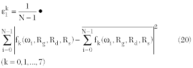
Moreover, for stable calculation, the discrepancy between the measured and calculated S-parameters is considered as a loose constrait. The mean values of intrinsic elements are used to calculate the S-parameters.
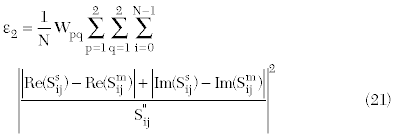
where
Ss= Modeled S-parameters
Sm=Measured S-parameters
Wpq (Fixed at 0.25)=Weight Factors
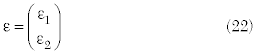
The extended error vector is then composed as follows:
Extraction Process

Figure 2 Flow chart of the iterative process.
A flowchart of the iterative process is shown in Figure 2. First, the initial extrinsic resistances and substrate elements are subtracted from the Z-parameters. The reduced Z-parameters are then converted to Y-parameters and the values of intrinsic elements are determined using Equations 14 to 19. Next, the extended error vector ε is estimated from Equation 22. The values of Rg, Rd and Rs are updated to reduce ε using the Powell method.
Experiment

Figure 3 Cgs frequency characteristics (Vds = 1.0V).
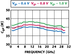
Figure 4 Cgd frequency characteristics (Vds = 1.0 V).

Figure 5 Cds frequency characteristics (Vds = 1.0 V).

Figure 6 Rds frequency characteristics (Vds = 1.0 V).

Figure 7 gm frequency characteristics (Vds = 1.0 V).
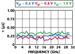
Figure 8 τ frequency characteristics (Vds = 1.0 V).
The MOSFET device has a channel mask length, L = 0.13 μm, a finger width, W = 5 μm, and a number of gate fingers, N = 16. Once the extrinsic elements are known, it is easy to determine the intrinsic elements for all biases. Figures 3 to 8 show the intrinsic elements dependence on the gate and drain biases.

The results show that the extracted parameters remain almost constant with frequency. However, it also can be found that frequency dispersion effects exist in the extraction of Rds and Cds. This verifies that those components are frequency independent and the method is accurate and reliable. Figure 9 compares the measured and modeled S-parameters for the MOSFET in the frequency range of 0.5 to 30 GHz under different bias conditions (Vds = 1.0, Vgs= 0.6, 0.8, 1.0). The modeled S-parameters agree very well with the measured ones.
Conclusion
An improved extraction technique for MOSFET small-signal model parameters is developed. The approach is based on a combination of analytical and optimization methods. ADS is then used to optimize only the parasitics with very small dispersion of initial values. Good agreement is obtained between the simulated and measured results over a wide range of bias points up to 30 GHz.
Acknowledgments
This work is supported in part by the Jiangsu Natural Science Foundation of China and Infineon Technologies.
References
1. S. Lee, C.S. Kim and H.K. Yu, “A Small-signal RF Model and Its Parameters Extraction for Substrate Effects in RF MOSFETs,” IEEE Transactions on Electron Devices, Vol. 48, No. 7, July 2001, pp. 1373-1379.
2. J. Gao, “An Approach for Determining PHEMT Small-signal Circuit Model Parameters up to 110 GHz,” International Journal of Infrared and Millimeter, Vol. 26, No. 7, July 2005, pp. 1017-1029.
3. G. Dambrine, A. Cappy. F. Heliodore and E. Playez, “A New Method for Determining the FET Small-signal Equivalent Circuit,” IEEE Transactions on Microwave Theory and Techniques, Vol. 36, No. 7, July 1988, pp. 1151-1159.
4. R. Anholt and S. Swirhun, “Equivalent-circuit Parameter Extraction for Cold GaAs MESFETs,” IEEE Transactions on Microwave Theory and Techniques, Vol. 39, No. 7, July 1991, pp. 1243-1247.
5. D. Lovelace, J. Costa and N. Camilleri, “Extracting Small-signal Model Parameters for Silicon MOSFET Transistors,” 1994 IEEE MTT-S International Microwave Symposium Digest, Vol. II, pp. 865-868.
6. G.J. Hu, C. Chang and Y.T. Chia, “Gate-voltage-dependent Effective Channel Length and Series Resistance of LDD MOSFETs,” IEEE Transactions on Electron Devices, Vol. 34, No. 12, December 1987, pp. 2469-2475.
7. I. Kwon, M. Je, K. Lee and H. Shin, “A Simple and Analytical Parameter-extraction Method of a Microwave MOSFET,” IEEE Transactions on Microwave Theory and Techniques, Vol. 50, No. 6, June 2002, pp. 1503-1509.
8. R. Torres-Torres and R. Murphy-Arteaga, “Straightforward Determination of Small-signal Model Parameters for Bulk RF-MOSFETs,” 5th International Caracas Conference on Devices, Circuits and Systems Proceedings, Vol. 1, November 2004, pp. 14-18.
9. K. Shirakawa, H. Oikawa, T. Shimura, Y. Kawasaki and T. Saito, “An Approach to Determining an Equivalent Circuit for HEMTs,” IEEE Transactions on Microwave Theory and Techniques, Vol. 43, No. 3, March 1995, pp. 499-503.