
In wireless handset design, specifically power amplifiers (PA), there is constant pressure to improve time-to-market while maintaining high yields. To meet these demands, designers need to evaluate current design practices and identify areas for improvement. Presently, most PA designers spend a great deal of time bench-tuning to optimize circuits. Since this is very time consuming, the main consideration is obtaining the best “nominal” performance, and process variation (or whether the wafer used for tuning is optimal) is generally an afterthought.
One common occurrence is that new circuit topologies are tried and minimal sample sizes are taken on a single wafer, often leading to “measured hero results.” However, once the design is run over many wafers, normal process variations may result in large performance changes that may give unacceptable yield levels. These variations are often blamed on the starting material or the fabrication process but, in reality, are usually due to expected process variations.

Including process statistics in the simulation phase would greatly reduce the occurrence of these frustrating events. However, implementation of statistical simulations in microwave designs (and III-V designs, specifically) is very limited, even though it is well established in the silicon (Si) digital or analog-mixed signal worlds. What are the barriers? The methodology used in the Si design community is usually built around Monte Carlo (MC) simulations.1-4 MC-based simulation is inherently time consuming, but necessary for most Si designs, where neighboring device mismatches are critical due to much smaller device sizes. The complicity and huge amount of time makes it “unfit” to III-V designs, where wafer turn-around time is much shorter (weeks rather than months, typical for Si designs). Si foundries may also provide “corner” models, but these are largely derived by driving figures of merit (like fT) that are not appropriate for most RF designs, where multiple criteria are to be met in one design. Some also provide customers with the option of wafer lots that capture the expected process variation (due to changing process variables),5 but do not provide a convenient way for customers to simulate exactly that set of wafers. Another major obstacle is the modeling approach of traditional GaAs devices, which is curve-fit-based rather than physics-based. The curve fitting makes it cumbersome, if not impossible, to provide a set of models that accurately tracks real-life process variations. Finally, most statistical analysis training focuses on using a particular software package, separate from the tool used for circuit simulation.6 This creates a barrier, since designers often do not have the time to learn another piece of software (or do not want to further fragment the design flow).
To overcome these barriers, several key considerations are offered in the development of a statistical-simulation-included designer-friendly design flow.
The approach should:
• Be predictive and approximate—real life examples (no non-physical variations are allowed).
• Be simple, convenient and faster than “trial-and-error.” Otherwise, it is viewed as an extra burden or nice “window dressing” for design reviews.
• Provide insight into what can be changed to make a better design, not just indicate how “poor” the design is. The simulation approach should be intuitive enough that designers can easily assess layout or design changes to reduce variation.
• Allow closure of the simulation loop by comparison with measurement of similar process spread wafers.
A design flow has been implemented, which takes advantage of the attributes of III-V HBT technology, by adopting a “unified” modeling approach and design-of-experiment (DOE) statistical simulation, selecting orthogonal only epi/process/operational variables, and using Advanced Design Systems (ADS) allowing high level integration of design, simulation and statistical analysis of a PA in a single tool.
Two examples are presented that significantly reduced circuit performance variation while maintaining the same nominal performance. These improved results demonstrate that with the same epi/process/operational specifications, the design topology and layout choices can obviously impact performance variation.
Since the DOE-based flow makes designers aware of process variation and allows the exploration before committing the design to GaAs, more process tolerant designs are achieved. This approach has resulted in the following benefits:
• The resulting designs are more robust and show less variation. This improved consistency allows customers to “set it and forget it” once these parts are used.
• These simulations are part of the design review to ensure that the design topology is solid. This provides some foundation for failure-modes effects and analysis.
• In the early stages of development, it has eliminated numerous circuit topologies that were terrible in terms of process variation.
• It provides guidance on future directions for process development and has allowed it to refine the Process Control Monitor (PCM) development (DOE simulation has been used on the PCM measurements to understand if the measurement is really measuring what is thought).
• It provides a tool to determine if a designer requests for tighter control on a parameter, such as beta, is reasonable or if there is another root cause for their variation.
• It is a valuable de-bugging tool (it can simulate how much variation is expected from one of the theorized causes). This is faster and easier than running the wafers or, at the very least, can guide what wafers get run. Simulation also helps eliminate other factors that may be the cause of the variation (so the need for a die level change or board level change is known).
KEY ELEMENTS OF THE APPROACH
The “unified” modeling and DOE simulation elements are based on the assumption that PA designs use large devices, so that device mismatch is negligible. The orthogonal-only-variables element focuses on further reduction of necessary simulation runs. The Pareto-drive really provides clear directions for designers on what to improve. Finally, the high level integration, everything into ADS, makes this design flow a powerful and practical tool for the III-V design community.
“Unified” Modeling
The unified modeling approach is the foundation of this design flow. It is a geometrical and physical modeling approach, which is described in more detail in the references.7,8 The term “unified” refers to the concept that devices fabricated from the same junctions or layers are forced to share, not only the same variation, but often the same model parameters.
For III-V HBTs technologies, front-end devices are formed by re-using junctions (base-emitter or base-collector junctions, etc.) or layers (emitter, base, sub-collector), and back-end devices (such as thin-film resistors, MIM capacitors and inductors) are independently formed but also share things like metal layers. The model parameters are separated into two sets: layout (geometry) dependent and material (epi) dependent. The geometry dependent parameters describing same type but different size devices, when varied, affect all devices of that type or sharing those layers equally. The geometrical dependence/variation is particularly important for resistor simulations. The material-dependent parameters allow to model the same geometry set of devices on a different epi by only changing a few parameters based on the specifics of the material design and drive variations across devices that share the same material layers, resulting in a greatly reduced total model/variation parameters for covering all devices in any given epi material.
A good example of this approach is shown in Figure 1, which illustrates how a semiconductor resistor (fabricated from the base layer of the HBT) model is constructed, and how it predicts the device behavior. In the model, the base sheet resistance is directly linked with a HBT parameter, ß, and the base-collector junction diode model is directly “borrowed” to the model topology to describe the underneath layer. This direct “borrow” and “link” approach, since it is physical based, characterizes the resistor electrical behavior very well.
How “Unified” Modeling is Different from Traditional Modeling Approach
In a traditional curve-fitting approach, different devices were modeled independently and little thought was given to consistency of the devices, such as HBTs, which did not share the model parameters with junction diodes or semiconductor layer resistors. In the extreme, the model parameters for the devices of the same type, say HBTs of different size or geometries, were not linked. As a result, it would take many parameters to vary each of these devices statistically on an individual basis, and some non-physical statistical states may be simulated.
Discussion on “Unified” Modeling and “Corner” Modeling
A simulation approach based on individual device corner modeling has been reported for some devices.9 That approach was only useful if there was only one design performance criteria, or for characterizing a system in which a single component really dominated the system behavior while other components’ variations were negligible, or when all the components varied independently (as if the parts were all independent discrete components). The possible statistical system responses, in these cases, could be obtained by simulating through the combinations of all the corners of all different devices being corner-modeled. However, for an MMIC, the assumption that circuit components vary independently, or that one device changes while other devices are constant are clearly incorrect. Adopting that approach would result in non-physical states and a lot of wasted effort worrying about variations that could never occur in reality.

This unified modeling approach is a physical corner modeling approach. It instantly generates corner models, by inputting statistical DOE parameters, which control all the on-chip devices together rather than individually and naturally guarantees physically possible circuit corner responses. It also requires less simulation iterations than running through different individual device corner models.
Statistical Variable Selection
For a GaAs HBT chip, there are many variables that can potentially be changed based on starting material or fabrication variation. For epi-variation, the models were implemented to allow individual material parameters (like doping and thickness) to be varied. However, for this work, model parameters are used (such as beta) that are actually responses to the doping and thickness.7 This link is necessary to help understand the circuit response (that is, it is important to know which parameter caused beta to change). As a result, only independent (orthogonal) epi and process variables, represented by model parameters, are made accessible for circuit statistical simulations, even though the orthogonality is not a requirement for general statistical simulation. The benefits are it minimizes the simulation time for the same circuit response one would get with more correlated variables and it eliminates any non-physical circuit responses of correlated parameters going in uncorrelated directions. The accessible parameters are listed in Table 1. The variations of the independent parameters are obtained from PCM data, which also provides the correlation parameters (based on material DOE runs)10 and validation of the orthogonality of the parameters.11 Reviewing the semiconductor resistor example again, instead of using both Rbsheet and ß variables to describe the resistor’s and HBT’s variations, only ß is made accessible (but Rbsheet changes according to ß inside the model code) to simulation. The strategy is to catch as much variation as possible with as few parameters as possible. The circuit operational variables are set to be simulation parameters as well.

Fig. 4 The DOE Pareto driven design flow chart.
Another feature of this implementation is that all the statistical parameters can be easily fixed to their nominal values. This allows designers to skip simulations of parameters that are not important for their particular design (for example, why simulate Schottky diode variation if it is not used in your circuit?), which greatly reduces the total simulation time. The number of statistical parameters in a typical circuit simulation, after such a selection approach, is less than 10.

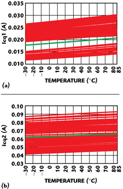
Fig. 5 Dual-band PA design using DOE simulation of Icq1 and Icq2.
DOE versus MC
The predicted mean and distribution ranges from MC depend on the number of variables and the number of simulations. The higher the ratio of simulation runs to the number of variables, the more accurate the predictions are. In reality, one normally does not really know which of the selected variables will have the most impact on a particular circuit design. Running hours of simulation to find this out is not very appealing. Worse, it could result in the most important parameters not getting selected because not enough simulation iterations were run. Both cases could lead to non-realistic distribution range predictions and less accurate mean predictions. DOE is widely used in the semiconductor industry. A short tutorial article to help readers understand DOE methodology is provided through the following link: http://www.agilent.com/find/eesof-doe.

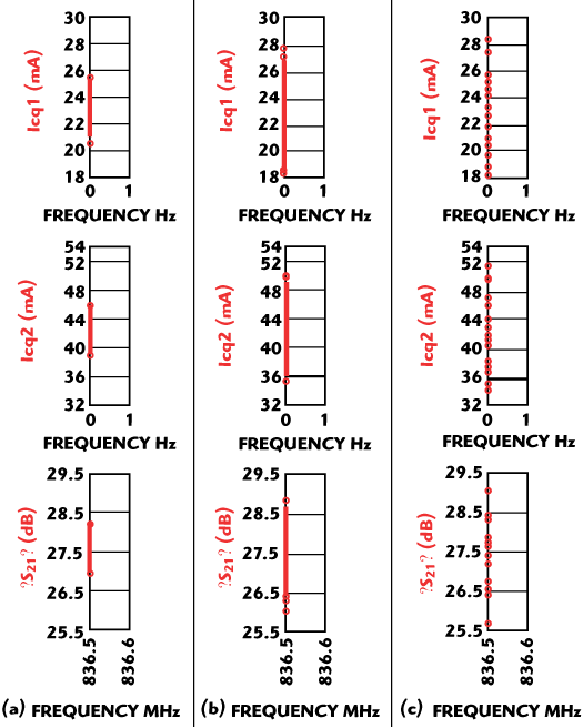
Fig. 6 Dual-band PA design using DOE simulation for gain.
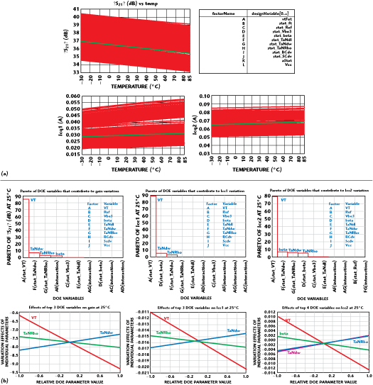
In the case that neighboring device mismatches are negligible, the study indicates that DOE is really an optimal simulation choice. Figure 2 shows in the situation of 4 variables, 64000 MC simulations led to much wider Icq ranges than that of 240 MC simulations. Since typical products ship in the millions, the ranges from 64000 MC simulations would be closer to accurately represent what really happens. However, 64000 MC simulations take 18.5 hours to finish while 240 simulations took only 470 seconds. The figure also shows that the results of a large number of MC simulations are required to approach the results of running a full factorial DOE simulation. The difference is that the DOE approach only took 28 seconds. To further investigate, the effect of each of the five variables involved in 250 runs MC and full factorial DOE simulation (25=32 runs) of another design was analyzed using JMP statistical software. The results are shown in Figure 3. The analyzed effects can be expressed by Equations 1 (MC) and 2 (DOE). Comparing these equations, it is obvious that the weight and direction of each variable from both results are identical. The main difference is the predicted means. As indicated earlier, this can be caused by using too few MC runs for the number of variables.


Fig. 7 Pareto charts for initial design; (a) Icq1 variations, (b) Icq2 variations and (c) gain variations.
Full Factorial DOE is Necessary
To refine the DOE approach, different DOE designs were studied. As seen in Appendix A, the full factorial DOE method (2kmp) gives consistent results with the much denser sampled 3k method, but takes much less time to run. The results of other DOE methods are not consistent with each other, even though they need a little less time than the full factorial method. The reason for the inconsistency of some other DOE methods is partly due to the orthogonal only (at device level) variable selection. The full factorial method is optimal, considering accuracy and simulation time, and was selected to be the method implemented in the design flow.
DOE versus “Sensitivity Analysis”
“Sensitivity Analysis” simulation is also evaluated. It predicts totally different results than the full factorial DOE and the dense sampled DOE (3k). The reason is that the “sensitivity” method only considers small perturbations around a nominal condition, with one parameter changed at a time. It is not a recommended method to improve design robustness.
Integrated Design Flow in ADS
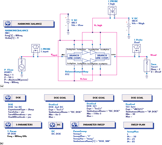
The fact that models, design circuits, DOE simulations and the instant simulation analysis are all integrated into ADS (see Sidebars 1 and 2) really makes the DOE design flow practical, even for those not so statistically savvy designers. In Sidebar 2a a few different circuit performances (the green lines) are displayed. The statistical state, for the performances where the markers are landed, is displayed as well. The markers on different performances plots are synchronized, that is when one marker on a particular measure is moved, the markers on other performance measures are automatically moved to indicate the performances of the same statistical state. Traditionally, statistical analysis, requiring special software and training, has been intimidating to many designers and has been one of the major barriers to its use in PA design.
The DOE Pareto Driven Design Flow
As shown in Figure 5, the integrated design flow consists of iterations of DOE simulations, reviewing circuit performances, reviewing Pareto charts, identifying circuit element corresponding to top Pareto factors for performance variation, and modifying the circuit. Once modified, the loop is followed until satisfactory results are obtained. The Pareto charts provide useful information about which variables dominate performance variation for the circuit. Such information is powerful for identifying which part of a design or specific component needs to be modified.

Fig. 8 Performance after modifications to reduce the impacts of top-order variables.
RESULTS
Dual-band PA
The first-cut design had wide Icq (see Figure 6) and RF gain (see Figure 7) variations. Pareto analysis showed that threshold voltage variations of the FET devices, width variations of some critical thin-film resistors, and DC gain variation of HBT devices were the dominant factors for the circuit performance variations (see Figure 8). To address these top-order effects, the internal reference voltage and values of three resistors were identified as the components to be changed. The performance variations were drastically reduced while the nominal performances are kept the same (see Figure 9).
WCDMA FEM
Battery voltage (Vcc) variations caused large circuit performance changes in the initial design (see Figure 10). Through the DOE Pareto driven design flow, insufficient ballasting and rising voltage on a particular node were identified as the root cause. As a result, clamping diodes and increased ballasting were implemented in the circuit. Some measured data verified that as Vcc changes from 3.2 to 4.5 V, Icq, after the design improvements, is relatively constant and the standard deviations are largely reduced at high Vcc. This example further illustrates the effectiveness of the DOE Pareto driven flow.


Fig. 9 Measured data for a WCDMA FEM design.
CONCLUSION
This work is the first one to integrate a unified modeling approach, DOE statistical circuit simulations of both epi/process and circuit operational variables, Pareto analysis, as well as design schematics into one design flow for a PA design. Each iteration of design modification is clearly driven by the Pareto-determined top-order variable, and the interactive process of design modification, simulation and obtaining feedback can be accomplished in a matter of minutes. It is shown how each key element in this system is determined to make this work distinct from all other statistical or design works. The examples of utilizing this approach demonstrate that much tighter performances can be achieved through modifying designs even if epi/process specifications are kept the same. Designers should have an active role in determining product robustness. As one can see, there are too many benefits to this approach to not adopt it.
ACKNOWLEDGMENT
The authors acknowledge model related discussions with Kai Kwok and Bin Li, and circuit discussions with Shiaw Chang and Andre Metzger. They also thank the several designers that acted as guinea pigs and helped refine this flow.
References
1. D.L. Harame, et al., “Design Automation Methodology and RF/Analog Modeling for RF CMOS and SiGe BiCMOS Technologies,” IBM Journal of Research and Development, Vol. 47, No. 2/3, March/May 2003.
2. W. Schneider, M. Schroter, W. Kraus and H. Wittkopf, “Statistical Simulation of High-frequency Bipolar Circuits,” 2007 Design, Automation & Test in Europe Conference & Exhibition Digest, pp. 1397-1402.
3. C.C. McAndrew, “Statistical Modeling for Circuit Simulation,” Proceedings of the Fourth International Symposium on Quality Electronic Design, 2003.
4. S.W. Director, et al., “Statistical Integrated Circuit Design,” IEEE Journal of Solid-State Circuits, Vol. 28, No. 3, March 1993, pp. 193-202.
5. W. Rensch, S. Williams and R.J. Bergeron, “BiCMOS Fab Yield Optimization,” IBM Microelectronics, First Quarter 2000, pp. 23-25.
6. J. Carroll and K. Chang, “Statistical Computer-aided Design for Microwave Circuits,” IEEE Transactions on Microwave Theory and Techniques, Vol. 44, No. 1, January 1996, pp. 24-32.
7. J. Hu, P.J. Zampardi, C. Cismaru, K. Kwok and Y. Yang, “Physics-based Scalable Modeling of GaAs HBTs,” Proceedings of the 2007 Bipolar Circuits and Technology Meeting, pp. 176-179.
8. P.J. Zampardi, “Modeling Challenges for Future III-V Technologies,” Workshop on Compact Modeling for RF-Microwave Applications (CMRF), Boston, MA, October 3, 2007.
9. N. Lu, “Statistical Models and Frequency-dependent Corner Models for Passive Devices,” 9th International Symposium on Quality Electronic Design Digest, 2008, pp. 543-548.
10. P.J. Zampardi, D. Nelson, P. Zhu, C. Luo, S. Rohlfing and A. Jayapalan, “A DOE Approach to Product Qualification for Linear Handset Power Amplifiers,” 2004 Compound Semiconductor Mantech Conference Digest, Miami, FL, pp. 91-94.
11. J. Hu, P.J. Zampardi, H. Shao, K.H. Kwok and C. Cismaru, “InGaP-GaAs HBT Statistical Modeling for RF Power Amplifier Designs,” Digest of the 2006 Compound Semiconductor Integrated Circuit Symposium, San Antonio, TX, pp. 219-222.