
Ultra-fast 100 GHz electrical sampling gates (“samplers”) with aperture widths of 7 picoseconds, and pulse generators (“pulsers”) with usable output energy extending to over 150 GHz, have both recently been demonstrated using a new, low-cost, fully monolithic “Rapid Automatic Cascode Exchange” (RACE) IC circuit architecture.1 These samplers, cast in Indium Phosphide (InP) DHBT and SiGe HBT IC processes, achieve comparable bandwidths to expensive hybrid sampler/pulser approaches, but with higher repetition rate and greatly reduced cost, size and power. This circuit architecture’s minute size further allows integration of multiple inherently-matched samplers and pulsers on a single IC, enabling small, low-cost microwave system solutions in ultra-wideband (UWB) communications, radar, satellite up- and down-conversion, network/spectrum analysis and spectroscopy, direct RF synthesis and acquisition, time-gated imaging and near zero-cost physical layer (PHY) analysis integrated into networking chips.
Electrical sampling gates (samplers) are widely used in oscilloscopes and other test equipment to capture high frequency signals, by providing brief (several picosecond wide) snapshots of an external signal. Present sampling oscilloscopes have input bandwidths of up to 100 GHz, but generally rely on costly samplers using a hybrid construction containing a step recovery diode (SRD) or nonlinear transmission line (NLTL) driving a Schottky diode pair.2–5 Similarly, microwave electrical pulsers, operating in essentially the reverse direction to that of samplers, generate narrow (multi-picosecond) pulses or sequences of repeating pulses (pulse trains), which result in broad frequency combs usable for time domain reflectometry (TDR) or transmission (TDT), network analysis, frequency up-conversion, radar and other applications requiring generation of signals with microwave frequency content in response to a lower frequency oscillator. Pulse trains with frequency content above 40 GHz also traditionally use SRD, NLTL and other methods whose high cost and modest repetition rates limit their use to only a subset of the applications in which pulsers and samplers could ultimately be used.
 Fig. 1 Train of 8 ps wide pulses with 2 ns spacing (green trace) produced by monolithic RACE pulser, and viewed by RACE sampler on same InP DHBT IC. Spectral plot is resulting frequency comb with 500 MHz tooth spacing to 142 GHz. Fundamental -8 dBm 500 MHz frequency peak at very left is superimposed 500 MHz externally inputted sine wave.
The recently developed low-cost monolithic RACE dual-function sampler and pulser ASIC circuit architecture (US Patent 6,433,720),1 described herein, enables the generation of pulses or sampling apertures in the 5 to 30 picosecond FWHM range with usable bandwidths over 100 GHz (as shown in Figure 1), repetition rates up to 20 billion pulses or samples per second and jitter too low to measure with most test equipment. This all-transistor architecture, invented by Furaxa Inc., and proto-typed jointly with the Naval Research Laboratory (NRL) in several IC technologies, including InP HBT and DHBT, SiGe HBT, GaAs and CMOS/SOI, eliminates the need for integral insulating substrates and transmission lines. Requiring under 0.25 mm2 of chip area, these high repetition rate samplers and pulsers enable a variety of portable low-power microwave applications, including UWB, comb-generated AM, FM, PM and QPSK communications, radar, next-generation oscilloscopes, network and spectrum analyzers, and direct satellite up-conversion and down-conversion without the need for microwave local oscillators. Also, unlike SRD and NLTL-based devices, these sampler/pulser cells can be integrated into larger monolithic ICs including new CMOS and SiGe ICs with sub-volt transistor breakdown voltages.
The ability to produce up to 20 billion pulses or samples per second allows replacement of microwave mixer/YIG oscillator front-ends with low-cost, integrated multiple-sampler/pulser-based up-/down-converters for satellite and other microwave communications applications.
Finally, the tiny size and high impedance sampler inputs and pulser outputs allow a combined sampler/pulser cell to be located directly in the signal path, as effectively as a tiny lumped element inside a larger IC (e.g., FPGA, 10/100G Ethernet, PCI-express or other PHY chip) or PCB, allowing in-situ observation and stimulation of signal nodes without the loading and high frequency losses posed by the 50 ohm connector and cabling environment required with conventional TDR/TDT instruments, enabling near zero-cost on-chip TDR/TDT/signal-integrity measurements.
RACE SAMPLER/PULSER ARCHITECTURE
 Fig. 2 Simplified diagram of circuit architecture of Furaxa differential sampler/pulser cell (US Patent 6,433,720) and graph of control input waveform with resulting current phase and held sample output.
The basic sampler cell has differential signal inputs IN+ and IN-, a clock input amplified by a conventional differential cascode amplifier to generate a fast-slewing “Control” signal, a set of DC input voltages (Vdd, Vee, V3, V2 and optionally V1), and a pair of output terminals OUT+ and OUT-, as shown in Figure 2. Each clock transition generates a rapidly falling edge on signal “Control,” which is fed to the sampler cell in Figure 2. A single falling (or rising) edge on “Control” causes the generation of either an electrical pulse or sampling aperture, depending on the values of R1 and R2, and whether the two Chold capacitors are present.
The input to be sampled (IN+ minus IN-) is fed into a conventional differential transistor pair (Q1/Q2), with optional cascoding (Q3/Q4), whose outputs differentially sink current from the bottom two terminals of the Libove Cell consisting of Q5 through Q12. Initially, the Control signal is above threshold voltage V3, and all of the current from the input amplifier is discarded through the blue-labeled steer-off path consisting of the upper transistor pair Q9/Q10 on the right side of the switch matrix in Figure 2. No current flows through transistors Q7/Q8 and therefore no current flows to the output terminals. Next, as the control voltage begins to fall below voltage V3, the input amplifier currents flow through the left transistor pairs (red-labeled path consisting of Q5/Q6 and Q7/Q8) to the output terminals, initiating the sampling aperture or pulse. Finally, as Control falls below voltage V2, all of the input currents now flow through the second (green-labeled) steer-off path, consisting of the lower right transistor pair Q11/Q12, thereby extinguishing the pulse or sampling aperture. In this way, a very fast electrical pulse is generated by a single clock input edge. The pulser may alternatively be configured as a sampler by increasing the values of load resistors R1 and R2, and adding a hold-capacitor in parallel with each resistor, so that most of the pulse energy remains stored in the capacitors.
Additional circuitry (not shown) for a practical sampler includes a differential output amplifier for subtracting the voltages on the left and right hold capacitors to obtain a bipolar output voltage. Finally, charge dump circuitry is needed to discharge the hold capacitors prior to each successive sample. Operational details are discussed in US patent 6,433,720.1 These samplers/pulsers may be configured to produce a pulse or aperture on the input clock’s rising edge, falling edge, or both, enabling a pulse or sample repetition rate of either 1× or 2× the clock frequency. In the case where a sample or pulse is only desired on one clock edge, it is necessary to either temporarily turn off the current source I, or bring V3 below V2 just prior to the clock edge in which the pulse or aperture is to be suppressed. Finally, a practical sampler or pulser is more complex than the circuit in Figure 2. For example, when using bipolar transistors, it is necessary to have two Control voltages falling together, and each offset by about 0.7 V, so as not to saturate transistors Q5 and Q6.
MONOLITHIC INP IC IMPLEMENTATIONS
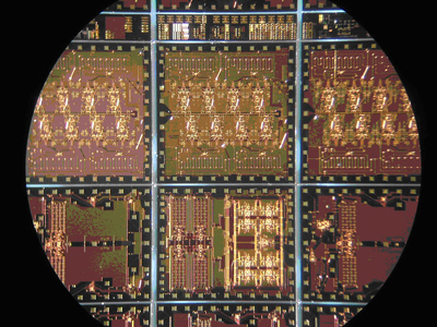
Fig. 3 Upper IC with 8 InP samplers and lower IC with 8 pulsers and integrated multiphase VCO.
An InP HBT IC containing eight 3 GSPS, 40 GHz bandwidth RACE samplers that deliver an aggregate 20 GSPS sampling rate is shown at the top of Figure 3. Such an IC could be used for low cost wideband oscilloscopes and network analyzers. Similarly, but operating in the opposite direction, the large IC at the bottom of Figure 3 contains eight 20 ps pulsers and an 8-phase monolithic voltage-controlled oscillator (VCO) (left side of IC), enabling ultra-wideband (UWB) Arbitrary Waveform Generation (AWG) at up to 24 GSPS.
PULSE GENERATOR AND SAMPLING GATE WITH 100 GHz USABLE BANDWIDTH CREATES TDR/VNA IN A SINGLE IC
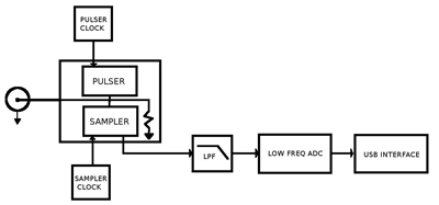
Fig. 4 Block diagram of a TDR sampling scope system having a common node (port) driven by a pulser and sampled by a sampler on the same IC.
Figure 4 is a block diagram showing an IC containing a pulser and sampler connected to a common pad that forms the microwave port. The IC is mounted on a PC board or substrate, and an external coaxial connector is connected to this node via a PC trace, and acts to the outside world as both a pulse-train output port and a sampler input port, effectively a time-domain reflectometer (TDR). The pulser and sampler are typically driven by separate clocks, with a small frequency offset (difference) between the two. The resultant output from the sampler is a convolution of the pulse (and its reflections and other input energy from the outside world) with the sample aperture. This relatively low frequency convolution waveform is periodic, with a repetition rate equal to the difference between the pulser and sampler clock frequencies and, after low-pass filtering, is digitized by an A/D converter interfaced to a computer.
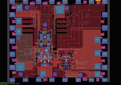
Fig. 5 100 GHz sampler (left) and pulser (right) in a single IC fabricated on InP DHBT.
Fabricated using the Agilent DHBT InP foundry, the IC in Figure 5 is the fastest RACE sampler/pulser IC manufactured to date, enabling over 100 GHz TDR/TDT/VNA performance in a monolithic IC. This IC implements the common node sampler and pulser shown earlier in Figure 4.

Fig. 6 Time domain plot from 100 GHz InP IC showing two successive pulses, 2 ns apart, with reflected pulse from open jack 200 ps after each incident pulses. Amplitude is approximately 500 mV peak. Horizontal scale is 250 ps/div. (middle, unwanted bursts are due to layout flaw).
A time domain waveform produced by the RACE pulser in the InP IC of Figure 5, and sampled by the RACE sampler on the same chip, is shown in Figure 6. Pulse repetition rate is equal to the pulser input clock frequency, which is 500 MHz (2 ns between pulses). A positive reflection from the un-terminated common port TDR jack (left silver connector in photo inset) results in a smaller peak occurring approximately 200 ps after each incident pulse. The sampling rate is equal to the sampler clock frequency of 499.9674 MHz, resulting in a convolution TDR waveform repeating 32,600 times per second. The displayed width of each pulse, convolved with the sample aperture’s transfer function, is approximately 10 ps, implying, due to the use of similar circuitry in both sampler and pulser, that the actual pulse width and sample aperture are each roughly 7 ps.
Figure 1 shows both the time domain waveform (green trace) and frequency spectrum (yellow trace) of the same RACE sampler, sampling the IC’s pulser output, but with the addition of a 500 MHz sine wave externally fed into the common port. The green time domain waveform trace shows the 500 MHz, -10 dBm sinusoidal signal along with the superimposed ultra-short sharp vertical pulser-output pulses. The yellow -10 dBm spectral peak at the left of the display is the amplitude of the 500 MHz sine wave, while the remaining 279 comb teeth are due to the repeating 500 MPPS pulse train. Averaging of the waveforms is done so that the entire 142 GHz spectral display is accumulated and updated approximately every two seconds. With this averaging, the noise floor is approximately 108 dB below the reference level.
Note that the decline seen in comb amplitude as frequency increases represents the combined pulser-sampler response, i.e. the declining pulser energy spectrum multiplied by the declining sampler sensitivity at high frequencies. Since the pulser and sampler have similar circuit topologies, we can roughly infer that each contributes to the decline in response to a similar degree. Therefore, the individual response of either the sampler or pulser declines at only half the rate of the combined response shown in Figure 1. For example, while the combined response at 102 GHz is 30 dB down from that at 1 GHz, the individual response of the pulser (or the sampler) can be inferred to only decrease by approximately 15 dB at 102 GHz.
The 100 GHz frequency response of both the sampler and pulser on this InP IC greatly exceeds the capabilities of the 50 GHz 2.4 mm coaxial connectors used on the test PC board, resulting in significant ripples in the frequency response of the resulting TDR. Such limitations could be addressed by upgrading to 1 mm connectors, or by directly feeding the sampler/pulser port into a suitable broadband microwave antenna, depending upon the application.
In this IC, pulses and samples are only produced on the falling clock edge, but due to a design defect, some pulse energy is also visible on the rising clock edge. This is visible on the green time domain traces of Figures 1 and 6, and by a serration of the comb in the frequency domain.
PULSE GENERATOR AND SAMPLER WITH 50 GHz USABLE BANDWIDTH IN A LOW-COST SiGe IC

Fig. 7 Time and frequency plots of SiGe RACE sampler/pulser IC with two pulses per 990 MHz clock, sampled by on-chip dual-comb sampler. 990 MHz peak at far left is from superimposed 990 MHz sine wave input. Serration of comb is due to mismatch between pulses generated on negative and positive edges.
While the InP ICs have yielded the highest speed, for many applications, a lower cost process is desirable. Multiple sampler and pulser ICs in a SiGe process have therefore been fabricated. Figure 7 shows a special “dual-comb” RACE sampler IC producing usable bandwidth to 50 GHz. This IC contains two identical halves, each containing two samplers and a pulser. One sampler in each pair acquires a sample on the rising edge of the input clock, the other on the falling edge of the input clock, resulting in a sampling rate that is twice the input clock frequency. This composite sampler therefore is receptive to a frequency comb with tooth spacing that is twice as wide as that of a single sampler. Also, by connecting the differential sampler outputs from the two samplers together either in phase or out of phase, the resulting frequency combs can be made selective to even or odd multiples, respectively, of the sampler input clock.
NEW APPLICATIONS ENABLED BY RACE SAMPLERS AND PULSERS
New InP DHBT, SiGe HBT, CMOS/SOI and GaN IC technologies, in combination with the RACE architecture, enable samplers and pulsers to be used in place of larger, costlier hybrid solutions, and could replace microwave tube assemblies in some applications.
The following section explores several applications recently prototyped, as well as potential future devices that could be rendered cost effective through the use of RACE sampler/pulsers.
Application 1: Concurrent stimulus, response and impedance measurements: Injection-locking a 14 GHz VCO while simultaneously observing the operation and output impedance

Fig. 8 GPPS Furaxa InP TDR pulser IC with on-chip 40 GHz BW, 0.999 GSPS TDR sampler and 14 GHz output of VCO injection-locked to TDR pulser.
Figure 8 shows a circuit board containing an InP HBT IC with two independent TDR-TDT channels, each comprising a 40 GHz InP sampler and a 10 ps pulser. The input of each sampler is connected to the same node as a pulser output and brought out to a 2.4 mm RF connector as a TDR port. The resulting instrument features a 14 ps reflected pulse width capable of very high resolution TDR or TDT measurements. In the application shown, a pulser is driving the output of an external 14 GHz SiGe VCO (board at top of photo), and injection-locking its output, while the sampler on the same channel is observing both the TDR response of the pulser and the 14 GHz VCO output. The positive-going pulse at the left of the scope display is the incident pulse, and the negative-going pulse 6 divisions later is the inverted pulse reflection from the low impedance of the VCO’s emitter-follower output. In this way, output impedance and signal output from a source are concurrently measured. The (quantity 14) low-level oscillations between the positive impulses (with 1 nanosecond period) is the sampled VCO output. A low-cost 1 GHz oscillator thereby down-converts a 14 GHz RF signal, providing an IF output within the bandwidth of a low-cost oscilloscope.
Application 2: Pulser-based arbitrary waveform generation

Fig. 9 Generation of modulated UWB burst waveform at 8 GPPS, using a GaAs 8 pulser module.
A microwave arbitrary waveform generator (AWG) synthesizing UWB bursts is shown in Figure 9. Pulse repetition rate is 8 GPPS. The burst shown is made up of 8 pulses, spaced 125 ps apart. Dynamic modulation and spectral shaping may be facilitated using D/A converters modulating the amplitude of each pulse. Bipolar microwave waveforms of any shape are thus produced.
Application 3: Low-cost universal front-end with pulser/sampler-based up- and down-conversion
The low repetition rate, high cost, and hybrid construction of prior art microwave samplers and pulsers has precluded their use in applications in which sampler-based systems would otherwise outperform microwave oscillators/mixer combinations. Rather than using expensive and large 10 to 100 GHz oscillators for up- and down-conversion, it is now possible to use a lower-cost 2 to 5 GHz coaxial resonant or SAW-stabilized oscillator clocking a high-repetition rate monolithic sampler or pulser to implement the equivalent respective down-conversion or up-conversion. The RACE architecture’s high repetition rate now facilitates these applications in a scalable, cost-effective manner. For example, very low-cost, single-chip vehicular radar, satellite up-/down-converters and direct microwave synthesizers are now feasible.
A low-cost multiple-sampler or multiple-pulser IC could replace mixers entirely in some applications, and still use an LO frequency that is a fraction of that of conventional microwave oscillators. However, a sampler-based front-end is generally noisier than a mixer-based down-converter, due to sensitivity to noise occurring at the frequencies of those sampler comb teeth outside the band of interest. Fortunately, we can take advantage of the ability to have multiple near zero cost RACE samplers and pulsers on a single IC to compensate for this, as explained below.
A pulser producing 4 billion pulses per second will generate a frequency comb having energy at 4, 8, 12, 16 GHz, etc., where the energy of successive teeth generally declines as frequency is increased. The rate at which the energy declines with increasing frequency is inversely proportional to the pulse width. Narrower pulse widths contain less energy, but spread that energy over a wider frequency range. Wider pulses contain more energy in the early comb teeth, but fall off more rapidly as frequency is increased. The same is true for samplers.

Fig. 10 Universal satellite band up/down-converter front end using two pulsers and two samplers.
A sampler, acquiring 4 billion samples per second, and followed by a low-pass filter, will be receptive to frequencies in the vicinity of 4, 8, 12 GHz, etc. However, it is necessary to reject the input at all but the desired comb frequency and, even with the wide spacing between adjacent comb teeth, large high-order filters may be required, potentially making samplers less desirable than mixers. Moreover, even if it were possible to filter out the energy in the adjacent comb teeth, a sampler-based receiver would still be receptive to internally generated noise at these unwanted frequencies, making its performance inferior to a mixer-based receiver. However, as shown in Figure 10, two inherently matched samplers and two inherently matched pulsers can be integrated on a single monolithic IC, connecting their common nodes to an output pad to drive an external bandpass filter and antenna. One pulser is clocked (made to produce a pulse) on the positive edge of the input clock, while the second is connected to produce a pulse on the negative edge of the clock, as shown in the left portion of the circuit of Figure 10.

Fig. 11 Wide comb-tooth spacing due to use of odd and even comb sampler pulser architecture.
Then, depending upon whether the differential outputs (or signal inputs) of the two pulsers are wired in phase, versus in opposition, the dual pulser combination will produce a frequency comb with, respectively, only even frequency comb teeth or odd frequency comb teeth, as illustrated in Figure 11. Now, even with a low 4 GHz input clock frequency, the successive comb teeth in the pulser’s output spectrum are spaced a full 8 GHz apart, which benefits the user by 1) concentrating all of the output energy in half as many comb teeth and 2) making rejection of adjacent comb teeth much easier, as they are spaced twice as far apart. Similarly, the dual samplers concentrate all of their sensitivity into half as many comb teeth, eliminating noise contribution from the unneeded comb tooth frequencies.
Future Applications
New applications enabled by the architecture include:
• Satellite up-/down-conversion without the need for microwave oscillators
•: High-impedance, non-intrusive in-line TDR/TDT and eye-pattern PHY measurements for serial buses, such as PCI-e, 10/100Gb Ethernet, SATA, Infiniband
• Medium power GaN or SiC radar, Tx/Rx IC
• Matched filters for microwave receivers
• Vehicular radar and intrusion detection
• LPOI/LPOD UWB transceivers with spectral shaping
• Ultra-low power UWB RFID tags
• Direct chip-to-chip communication using UWB pulses, replacing PCB traces
• Low cost spectrum and vector network analyzers
• Microwave monolithic sampling phase detectors
• Time gated microwave medical imaging systems
• Driver for terahertz diodes for explosives detection and other spectroscopy
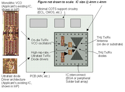
Fig. 12 Concept for low-cost THz spectrometer IC using RACEs and a THz diode/antenna assembly.
The RACE’s monolithic nature, multi-GHz repetition rate and narrow pulse width could enable the construction of low-cost Terahertz (THz) spectrometers.6,7 Figure 12 shows a proposed THz spectrometer using two RACE pulsers driving a THz diode/antenna assembly on a single IC. The pulses from the InP RACEs are fed to a bridge of THz Schottky diodes, which produce a sharpened pulse, due to their abrupt conduction. This pulse contains energy up to 1 to 2 THz, which is transmitted by a small antenna. The signal received back from the antenna is sampled by a similarly-pumped sampler containing two THz Schottky diodes, with a very narrow resulting aperture. Potential applications include IED detection, through-wall radar, airport and entry point screening spectrometers, and blood chemistry measurement.
LIMITATIONS AND FUTURE IMPROVEMENTS
As with all samplers, RACEs exhibit harmonic and intermodulation distortion, as well as amplitude-dependent sampling point position modulation. While RACEs exhibit low noise, superior speed and ultra-low cost, the linearity of uncompensated RACE samplers is only fair, with low frequency second and third harmonic distortion down by approximately -45 and -60 dB, respectively, in present implementations. Also, as with pre-existing electrical samplers, the actual sampling point position time-shifts (by about 0.2 ps) when changing from acquiring a 0 V signal to acquiring a full-scale signal. Both of these phenomena are deterministic and can be compensated for using analog or digital methods. One simple way to linearize and time-compensate samplers is with FPGA or DSP-implemented look-up table-based algorithms. Future RACE ICs could also contain analog pre-distortion and pre-compensation circuitry to correct for the two problems. Finally, while not a problem with a RACE sampler (whose sampled outputs contain only moderate frequency content), a RACE pulser’s differential pulse outputs are unipolar, so to create a bipolar output pulse, one needs to use a microwave balan or differentially fed antenna to subtract the two unipolar outputs. As RACE pulsers’ output pulses are faster than any differential amplifiers the authors have been able to design, a balanced passive load is preferred, to perform subtraction at sufficient speed to preserve the very high frequency content the pulser can generate.
CONCLUSION
A novel sampling and pulse generating technology has been implemented in InP, SiGe, GaAs and CMOS IC processes, and has demonstrated lower cost and improved operation over existing architectures. Early results were presented, and promising current and future applications were proposed for this enabling technology.
References
1. J.M. Libove and S.J. Chacko, “Methods, Apparatuses and Systems for Sampling or Pulse Generation,” US Patent 6,433,720, August 13, 2002.
2. K.B. Magleby and W.M. Grove, “Signal Sampling Circuit Including a Signal Conductor Disposed in the Electromagnetic Field of a Shorted Transmission Line,” US Patent 3,241,076, March 15, 1966.
3. L.R. Lockwood, “Phase Detector,” US Patent 4,654,600, March 31, 1987.
4. R. Landauer, “Parametric Amplification along Nonlinear Transmission Lines,” Journal of Applied Physics, Vol. 31, No. 3, March 1960, pp. 479–83.
5. M.J.W. Rodwell, et al., “Nonlinear Transmission Line for Picosecond Pulse Compression and Broadband Phase Modulation,” Electronics Letters, Vol. 23, No. 3, January 29, 1987, pp. 109–110.
6. P. Siegel, “Terahertz Technology,” IEEE Transactions on Microwave Theory and Techniques, Vol. 50, 2002, p. 910.
7. J. Ward, E. Schlecht, G. Chattopadhyay, A. Maestrini, J. Gill, F. Maiwald, H. Javadi and I. Mehdi, “Capability of THz Sources Based on Schottky Diode Frequency Multiplier Chain,” IEEE MTT-S International Microwave Symposium Proceedings, Fort Worth, TX, June 2004, pp. 1587–1590.
Joel M. Libove received his BSEE degree from Cornell University and his MSEE and PhD degrees from the University of California at Berkeley. He holds 17 patents, and has published in the areas of high-speed electronics, non-contact voltage measurement, medical instrumentation and computer bus automatic fault recognition tools. He is president of Furaxa Inc. and chairman of Ultraview Corp.
Brendan R. Illingworth received his BSCE and BSMA degrees from the University of California at Santa Cruz and his MSCES degree from Sonoma State University. He is the lead design engineer for analog IC and FPGA projects at Furaxa.
Steven J. Chacko received his BSEE degree from California Polytechnic in San Luis Obispo, his MSEE degree from Stanford University and his MBA degree from the University of California at Berkeley. He has over 14 years of experience in R&D, marketing and management at Hughes Aircraft, ViaSat and S5 Wireless. He has successfully developed and marketed products for military and commercial applications in satellite and terrestrial communications, and is co-inventor of several patented technologies.
Hal L. Levitt received his BS degree in electrical engineering and his MS degree in applied physics. He is a supervisory engineer within the Tactical Electronic Warfare Division of the Naval Research Laboratory, Washington, DC. He currently specializes in development of miniature electronic warfare receivers for remote sensor applications. He holds seven patents in the areas of optical and electrical signal processing.