
Baseband digital predistortion (DPD) is an attractive method to improve the performance of high power amplifiers (PA). The feedback loop plays a very important role in the baseband DPD system. Its aim is to obtain the sampled signals on which the model of the PA is based and the DPD processing is done. The imperfections of the devices in the analog circuits, such as the modulator and demodulator, will influence the signal performance. Such non-ideal characters will influence the modeling of the PA and the processing of the DPD part and therefore limit the improvement of the predistortion system. In this article, error items of the modulation and the demodulation in the feedback loop are analyzed and the compensation and correction algorithm is derived. Simulations are accomplished to validate the closed-form algorithm in a numerical way. The compensation and correction of the errors can be carried out automatically, and this method can be easily adopted in the adaptive DPD based on real-time data.
Advanced current and future mobile communication systems are required to achieve very high data rate to make the broadband applications realizable. Therefore, complicated digital modulation techniques such as 16QAM and 64QAM are adopted in such systems to enhance the spectrum efficiency. Accordingly, power amplifiers built in the base stations of those systems need to be characterized for high linearity and efficiency to meet the large peak-to-average ratio of the high order digital modulated signals. Linearization techniques such as the feed-forward method, radio frequency (RF) predistortion method and digital predistortion method are usually used to enhance the linearity and the efficiency of the power amplifiers.
For the feed-forward linearization method,1 it is quite difficult to control precisely the amplitude and phase of the compensating RF signals added to the original distorted signals. For the RF predistortion linearization method, the inverse functions of the power amplifiers are difficult to realize exactly, which will limit the linearity improvement. Baseband digital predistortion linearization methods based on a LUT table2 or PA behavior models3 modify the baseband signals directly to ameliorate the linearity of the amplified RF signals. In order to explain the error analysis more clearly, a simplified block diagram of a typical digital predistortion system4 is shown in Figure 1.
The procedure for the DPD has been described previously.2 During the training stage, the digital DI1 and DQ1 data of the training signals are converted to the analog AI1 and AQ1 signals by the DACs. The I and Q signals are then modulated to the RF band by a direct quadrature modulator. The modulated signal is sent to the driver amplifier and the power amplifier under the test and linearization. The amplified and distorted signal is coupled into the down converter and is then demodulated to baseband I4 and Q4 signals. ADCs are used to digitalize the I4 and Q4 signals. By comparing the original DI0 and DQ0 data and the digitalized DI4 and DQ4 data, the nonlinearity of the power amplifier can be estimated, based on which the digital predistortion can be realized. The mechanism of the predistortion is to change the characteristics of the baseband signals to compensate the distortion caused by the power amplifier in advance.

Figure 1 Simplified diagram of the baseband digital predistortion
It is obvious that the modulator and the demodulator are very important devices in the predistortion feedback loop. Imperfect modulators and demodulators will cause some additional distortions to such a system. Some of these distortions, arising in the feedback route, should not be regarded as the congenital characteristics of the power amplifier.
The effects of the imperfection of the modulation and demodulation have been noted in different ways,5–8 but without compensation. Some compensation methods based on an envelope detector (ED) have been introduced.9 These methods are quite complicated and an ideal ED and an ADC must be used additionally for estimation. Because the output of the ED is a scale value, many input data and complex data processing are needed for accurate estimation.
However, in adaptive DPD systems, the feedback loop provides vector values of the coupled PA output. To estimate the model of the PA or DPD, these feedback vector data are very useful for fast and accurate estimation of the quadrature modulator and demodulator error.
In this article, the effect of the modulation and demodulation imperfection on the modeling of the power amplifiers and DPD processing are analyzed. To overcome the unwanted effect of those errors, straightforward estimation and compensation algorithms are derived to achieve the ideal modulation and demodulation data. With the method described in this article, no additional EDs and ADCs are required. The effect of the correction and compensation is verified by the subsequent detailed simulations. This adaptive compensation method is easy to realize and can be embedded in adaptive DPD systems.
ERROR ANALYSIS, DERIVATION AND SIMULATION
The feedback loop is an important unit in the DPD system. Modulators and demodulators are the key components of the feedback loop. They convert the analog baseband I and Q signals to the RF band and convert the coupled output signals to the analog baseband I and Q signals. Since signals transmitted from the base stations are normally band limited and with few spurious emissions, direct modulators and demodulators are adopted here to simplify the feedback loop structure. According to the sampled feedback signal data with the nonlinear distortion and the directly sampled baseband signals data without nonlinear distortion, the predistortion data used to modify the digital baseband signals can be obtained.

Figure 2 Analog quadrature modulation and demodulation.
The quadrature modulation process of the transmitting path and the quadrature demodulation process of the feedback path can be simplified, as shown in Figure 2. Here, Ψ is the signal phase shift on the RF channel between the transmitting and receiving ports. It is a determinate value caused by the passive coupler, microstrip lines, amplifiers, etc., which can be estimated and compensated at the receiving end.
If the modulator is an ideal one, which means the amplitude error and phase error are zeros, and assuming that the PA is an ideal linear amplifier with linear gain APALI, the modulated signal fed to the demodulator is

where
A1 = amplitude gain of the quadrature modulator
φ1 = phase shift caused by the modulator
The coupling coefficient of the coupler is assumed to be 1 for simplicity. Such direct modulation and radio channel transmission can be presented using equivalent baseband modulation for efficiency, which can be expressed as

If the modulator is also an ideal one, the output of the ideal demodulator after the low pass filter is

where
A2 = amplitude gain of the quadrature demodulator
φ2 = phase shift caused by the demodulator
Such demodulation can also be equalized to baseband demodulation, which can be expressed as

However, available quadrature modulators and demodulators are not ideal devices.10 The amplitude and phase errors of modulators and demodulators will introduce additional distortions to the modulated and demodulated signals. The amplitude error of the modulator or the demodulator is the amplitude difference between the in-phase and quadrature paths of the modulator or the demodulator. Similarly, so is the phase error. Assuming that the amplitude and phase errors of the modulator and the demodulator are ΔA1, ΔA2, Δφ1 and Δφ2, respectively, when the modulators and demodulators are non-ideal, Equations 2 and 5 should be rewritten as Equations 6 and 7


If the power amplifier is a linear transform, which is projected to baseband as APALI for simplicity, Equation 7 can be rewritten as

Therefore, error items in the received I4(t) and Q4(t) signals can be presented as

where
φc = φ1 - φ2 + Ψ
Ac = A1APALA2
Apparently, error items εI and εQ in Equation 9 include the non-ideal characters of the modulator and demodulator, which will cause the imbalance of the received I4(t) and Q4(t). Since building the PA model is essentially based on the I4(t) and Q4(t) from the feedback loop of the system, the εI and εQ will affect the accuracy of the model to some degree and will eventually limit the improvement of the linearity of the PA.
According to the simplified diagram of the baseband digital predistortion, the transmitting path includes the modulator, driver and PA, while the path of the training series includes the modulator, driver, PA, demodulator and the low-band pass filters. That is to say, the training signals not only carry the error information from the transmitting path, which the normal signals undergo, but also carry the error information from the feedback path, independent to the transmitting path. It seems that only the errors caused by the imperfection of the demodulation should be corrected additionally.11 In fact, since the errors caused by the modulation are added before the power amplifier, the imbalances are amplified nonlinearly and cannot be correctly compensated by the normal DPD solutions. Compensating the errors caused by both the quadrature modulation and the quadrature demodulation in the feedback loop will improve the performance of the DPD system. That is the purpose of this algorithm. Simulations are completed including the whole DPD platform using the polynomial model for power amplifiers.
Without Modulation and Demodulation Error
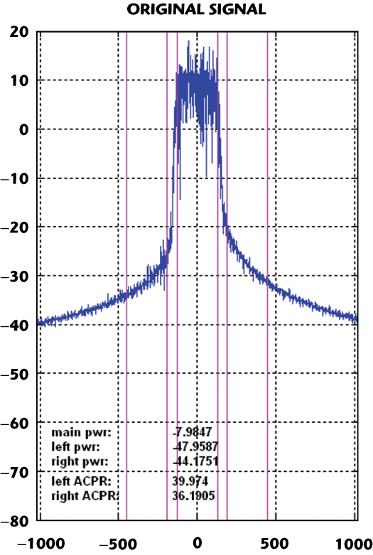
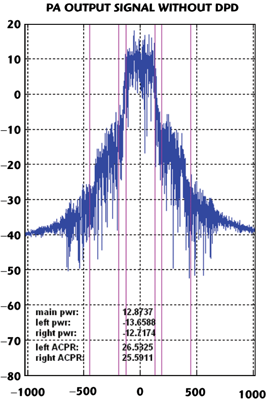
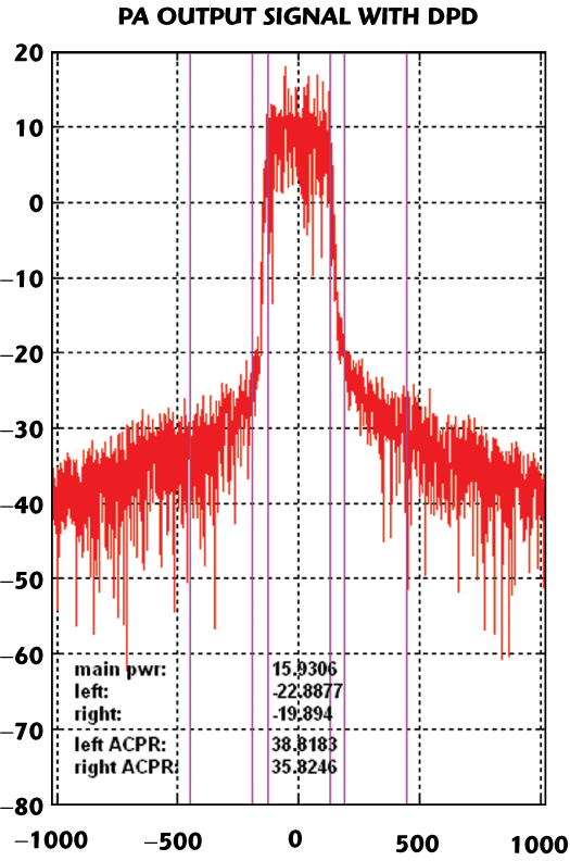
The original 16QAM modulated input signal of the PA, the PA output signal without DPD and the PA output signal with DPD are shown in Figure 3. The ARCTAN PA model12 in Equation 10 is used in the simulation and the memory-less polynomial model in Equation 11 is adopted to fit the PA model in the DPD processing unit.

where

γ1 = 8.00335 - j4.61157
γ2 = -3.77167 - j12.03758
ζ1 = 2.26895
ζ2 = 0.8234 from the data of RFIC PA12

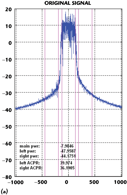
In the case of the polynomial order n is 9, the PA output signal with DPD processing is shown in the figure. The adjacent channel power ratio (ACPR) results of the original signal, the amplified PA output signal without DPD processing and the amplified PA output signal with DPD processing are listed in Table 1. It is obvious that without the modulation and demodulation errors, the ACPR of the amplified output signal with DPD processing is very close to the original linearity.

With Modulation and Demodulation Errors
Non-ideal modulator or demodulator characteristics are considered in this part of the simulation.
Effect on ACPR Performance

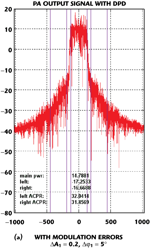
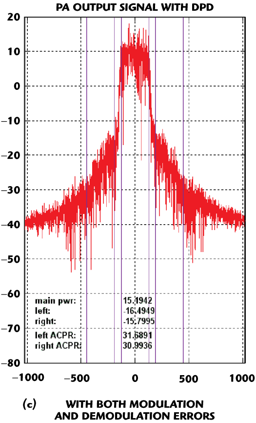
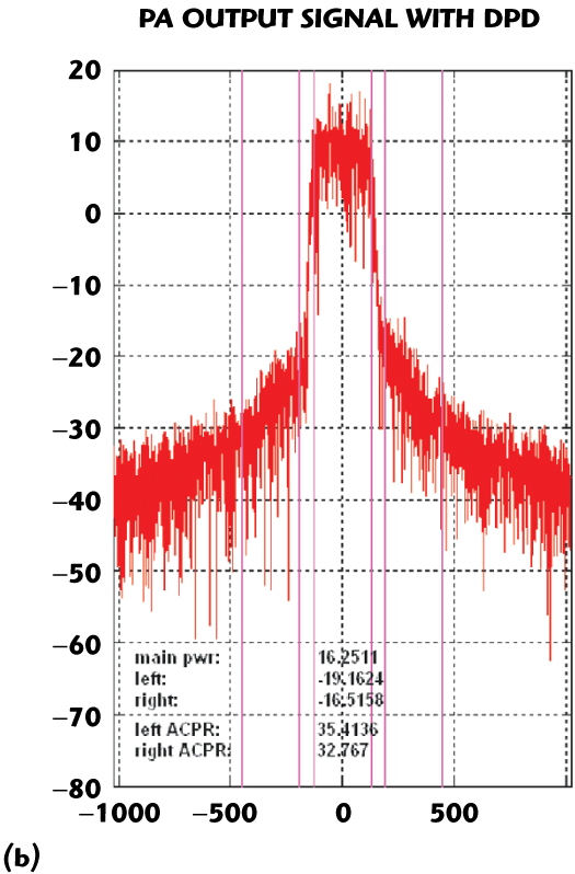
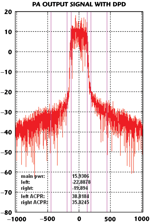
The effect of modulator imbalance on DPD improvement is shown in Figure 4(a), in the case of an amplitude error of 0.2 and a phase error of 5°. Similarly, the effect of a non-ideal demodulator is shown in Figure 4(b), in the case of an amplitude error of 0.2 and a phase error of 5°. And in Figure 4(c), the effect of both the modulation and demodulation errors is shown. Here, the polynomial order n is 7. The simulated results show that the DPD improvements are degraded significantly and the modulation error cannot be compensated in the DPD system. The ACPR results are listed in Table 2. From Tables 1 and 2, it is obvious that the ACPR performance in the DPD system is degraded by the existence of the modulation and demodulation errors. It seems that the degradation caused by the modulation errors is more significant, for the imbalances are amplified by the nonlinear PA.
Effect on PA Modeling
 Figure 5 Effect of modulation and demodulation errors on PA modeling.
In fact, the errors of the modulation and demodulation affect the modeling of the PA. Figure 5 shows the simulation results under different conditions. The order of the polynomial for the PA behavior model n = 9. Obvious departure can be observed.
Effect on the DPD Processing Algorithm Convergence
Adopting a higher polynomial order will give better fitting to the real PA input-output relationship curve. But the modulation and demodulation errors will cause the divergence of the DPD processing algorithm when increasing the order of the polynomial order.
 Figure 6 DPD output and PA output with DPD processing signals.
Figure 6 shows the DPD processing output data without and with modulation and demodulation errors
ΔA1 = 0.2
Δφ1 = 5°
ΔA2 = 0.2
and
Δφ2 = 5°
Both simulations are done under polynomial order n = 9. The DPD processing algorithm follows the Newton descent method, which has the property of rapid global convergence.
According to the figure, it is clear that the PA output line with DPD processing departs from the linear output line when modulation and demodulation errors exist due to the fact that the polynomial fitting curve is deflective. In this case, inaccurate polynomial coefficients give a higher input amplitude level limit and this will cause the divergence of the DPD processing algorithm. In this article, the PA output limit is used to avoid the instability.
ERROR CORRECTION DERIVATION, COMPENSATION AND SIMULATION
The estimation and compensation of the modulation and demodulation errors in the feedback loop of the DPD system will improve the PA modeling. These will be useful for the DPD algorithm to enhance the DPD performance.
System Structure
 Figure 7 Diagram of the modified baseband digital predistortion system.
The modified DPD system is shown in Figure 7. A modulation correction unit and a demodulation compensation unit are added into the feedback loop of the baseband DPD system. Accordingly, some testing signals generating units are added for automatic error estimation.
Correction and Compensation for the Demodulation Errors
In order to eliminate the error items of the nonideal demodulator, a test signal can be input into the feedback path to calculate the error parameters ΔA2 and Δφ2 of the demodulator. Supposing that an RF continuous wave signal stest(t) = cos(ωct - ωst) is fed into the feedback path at the test point indicated in the figure and assuming that during the test and self-correction stage, no other normal signals are fed into the receiving path, such interfering free conditions for test and self-correction can be realized by mechanical switching and software controlling. The received and demodulated signals in feedback path are


During the test and self-correction stage, the value arrays of I'Btest(t) and Q'Btest(t) can be obtained from AD converters in the feedback path. Therefore, using the Fourier transformation, A'1Btest(t), A'QBtest(t), α'1Btest, α'QBtest can be obtained and regarded as knowns, with which ΔA2 and Δphi;2 can be calculated with Equation 14.

With the calculated error parameters ΔA2 and Δφ2, a compensating unit can be inserted into the feedback path between the AD converters and predistortion processing unit as shown, where I'3(t) and Q'3(t) denote compensated signals.
According to Equations 5 and 7, the relations among I3(t), Q3(t), I'3(t) and Q'3(t) can be deduced and expressed in Equation 15. Therefore, the compensated or corrected baseband signals data arrays I'3(t) and Q'3(t) can be obtained from the I3(t) and Q3(t) data arrays.

After the compensation or correction, the imperfection of the demodulation will be eliminated.
Correction and Compensation for the Modulation Errors
After the demodulation errors are corrected, the modulation errors can be corrected by sending the test signals into the link from the processing center similarly. Any two unrelated known baseband signals can be sent for estimation. For simplicity, two testing signals in Equation 14 are adopted to extract the modulator error parameters ΔA1 and Δφ1

where Atxtest is small enough to make the power amplifier work in the perfect linear range.

According to Equation 8, the received testing signals from the AD converters in the feedback loop can be expressed as

Then, the error parameters ΔA1 and Δφ1 can be extracted from Equations 17 and 18.

According Equations 2 and 6, the relations among I0(t), Q0(t), I'0(t) and Q'0(t) can be deduced and expressed by Equation 20.

A modulation correction unit can be added to the loop before the modulator to compensate the modulation errors. Thus, by adding the correction and compensation units, the imbalance errors caused by the quadrature modulation and demodulation can be eliminated to improve the effect of the baseband DPD processing.
Correction and Compensation Effect
The complete simulations include the procedures of quadrature demodulation and modulation imbalance parameters extraction, quadrature modulation and demodulation, PA model establishing, DPD inverse-PA model establishing and calculation and DPD data processing.
Assuming that the errors items are
ΔA1 = 0.15
Δφ1 = 4°
ΔA2 = 4° 0.15
and

Δφ2 = 4°
• First, a test simulation case is done when the demodulation is not corrected. Without the compensation of the demodulation, the extracted error parameters of the modulation are Δφ1 = 0.2354 and Δφ1 = 8.0012°. Figure 8 presents the result of the modulation compensation without the demodulation correction. In this case, since incorrect error parameters are estimated and used for compensation of the modulation, the PA model is not accurately fitted and the DPD processing improvement is limited. The ACPR performances are -35.41 dBc at the lower adjacent channel and -32.77 dBc at the higher channel. It is clear that if the demodulation errors are not correctly compensated, the performance of the modulation compensation and DPD improvement will suffer from the errors of the demodulation.

• In the case of both the compensations are added for the quadrature modulation and demodulation, the results are excellent. The extracted error parameters of the modulator and demodulators are:
ΔA1 = 0.1500
Δφ1 = 4.0000°
ΔA2 = 0.1500
and
Δφ2 = 3.9993°


which are almost identical to the presumed parameters. The DPD processing results with modulation and demodulation compensations are shown in Figures 9a and 9b. The original signal is the same in both cases. The polynomial order is n = 9. The improved ACPR performance results are listed in Table 3. The simulation results show that the use of modulation and demodulation compensation has a very obvious effect in enhancing the linearity improvement of the baseband DPD system.
Generally, the modulation errors and demodulation errors vary slowly, and can be treated as constants for a quite long time period. The estimation of the demodulation error can be executed at the beginning of the DPD, or any time required, by switching the demodulation input to the RF testing signal. In fact, the error of the modulation can be calculated by adding two unrelated small signals to the modulator, letting the PA operate in the perfect linear region. Therefore, the estimation and compensation of the modulation can be executed adaptively in the normal operation state. The adaptive compensation method has good flexibility and can be modularized into adaptive baseband DPD systems.
CONCLUSION
In this article, quadrature modulated and demodulated signal components and error items are analyzed first. It is indicated that the performance of the modulation and demodulation will influence the amplitude and the phase balances of the signals; therefore, the modeling of the PA and the calculation and convergence of the DPD algorithm will be affected. Consequently, the linearity improvement, namely the DPD performance, will be obviously limited. Imbalanced items in the amplitude and phase of the quadrature modulation and demodulation are then calculated. The analytical relations between the original input and the compensated signals of the modulation and demodulation are derived, respectively. Complete simulations are carried out to realize the closed-form derivation with numerical calculations and the correction and compensation results are very good.
According to the analysis, derivation and simulation presented, the error items caused by the imperfect modulator and demodulator in the feedback loop can be eliminated and the corrected modulated and demodulated data can be obtained. In practice, testing signals are sent from the DPD processing unit. The additional compensating units, based on the algorithm and the method introduced in this article, eliminate the error items in the feedback data arrays that are introduced by both the modulation and demodulation process. This provides the DPD processing unit cleaner data arrays of the feedback training or normal signals to establish the PA model and the DPD processing. As a result, a more precise nonlinear model of the power amplifier can be obtained using curve fitting at the DPD processing unit. More accurate DPD processing results can also be calculated from the system. Therefore, the modified DPD system will get rid of the performance limit caused by the errors in the feedback loop and acquire more improvement on linearity. An adaptive baseband DPD system was introduced in a previous article,2 which is focused on the complex LUT scheme for PA model establishment. In the present article, it is based on the adaptive polynomial PA model. It is quite difficult to use the LUT method to deal with the memory effect of the PA, whereas the polynomial PA model is suitable for processing the memory effect. In advanced adaptive digital predistortion systems, the polynomial model and its extensions are widely used to accurately describe the behavior of the PA. Furthermore, that article did not include the error estimation and compensation unit. A great deal of tuning work has to be done to minimize the modulation and demodulation errors to obtain a good performance. Because the imperfection may slightly vary with the operating conditions, some degradation will be introduced when the conditions change. In the design described here, the estimation and compensation are carried out automatically in the digital domain and can start the calibration at any time. It is very suitable for adaptive linearization.
References
1. J. Zhou, L. Zhang, W. Hong, J. Zhao and X. Zhu, “Design of a Wideband Adaptive Linear Amplifier with a DSB Pilot and Complex Coherent Detection Method,” Microwave Journal, Vol. 49, No. 4, April 2006, pp. 104–114.
2. J. Zhou, S. Ming, J. Zhao, C. Ming and L. Zhang, “An Adaptive Baseband Digital Predistortion System for RF Power Amplifier: Design, Hardware and Software Realization and Experimental Test,” Microwave Journal, Vol. 50, No. 5, May 2007, pp. 216–220.
3. L. Ding, G.T. Zhou, D.R. Morgan, Z. Ma, J.S. Kenney, J. Kim and C.R. Giardina, “A Robust Digital Baseband Predistorter Constructed Using Memory Polynomials,” IEEE Transactions on Communications, Vol. 52, No. 1, January 2004, pp. 159–165.
4. M. Shi, M. Chen, L. Zhang and J. Zhou, “A New Baseband Digital Predistortion System,” 2005 Microwave Conference Proceedings (APMC), China, Vol. 2.
5. J.K. Cavers, “The Effect of Quadrature Modulator and Demodulator Errors on Adaptive Digital Predistorters for Amplifier Linearization,” IEEE Transactions on Vehicular Technology, Vol. 46, No. 2, May 1997, pp. 456–466.
6. Q. Ren and I. Wolff, “Effect of Demodulator Errors on Predistortion Linearization,” IEEE Transactions on Broadcasting, Vol. 45, No. 2, June 1999, pp. 153–161.
7. K.C. Lee and P. Gardner, “Effects of Demodulator Errors on Convergence Time of Look-up Table Based Iterative Algorithms for Adaptive Digital Predistortion Linearizer,” 2004 IEEE International Symposium on Circuits and Systems Digest, Vol. 1, pp. 425–428.
8. I. Teikari and K. Halonen, “The Effect of Quadrature Modulator Nonlinearity on a Digital Baseband Predistortion System,” 2004 European Microwave Conference Digest, pp. 1637–1640.
9. J.K. Cavers, “New Methods for Adaptation of Quadrature Modulators and Demodulators in Amplifier Linearization Circuits,” IEEE Transactions on Vehicular Technology, Vol. 46, No. 3, August 1997, pp. 707–716.
10. M.Y. Li, J.X. Deng, L.E. Larson and P.M. Asbeck, “Non-ideal Effects of Reconstruction Filter and I/Q Imbalance in Digital Predistortion,” 2006 IEEE Radio and Wireless Symposium Digest, pp. 259–262.
11. J. Zhao, J. Zhou, N. Xie, J. Zhai and L. Zhang, “Error Analysis and Compensation Algorithm for Digital Predistortion Systems,” 2007 Progress in Electromagnetics Research Symposium Digest (PIERS), Beijing, China, Vol. 2, No. 6, pp. 702–705.
12. R. Raich, H. Qian and G.T. Zhou, “Orthogonal Polynomials for Power Amplifier Modeling and Predistorter Design,” IEEE Transactions on Vehicular Technology, Vol. 53, No. 5, September 2004, pp. 1468–1479.