
During World War II, RF and microwave systems proved to be of major importance for both communication and radar. Consequently, intensive research was conducted in this field, resulting in major breakthroughs. The introduction of novel communication and sensing equipment continued after the war for both military and civilian applications. As a result, the frequency spectrum up to 10 to 20 GHz became increasingly crowded, thus limiting the introduction of new and advanced applications.
Ultimately, discussions came up quite early on the use of frequencies beyond 30 GHz, allowing huge bandwidths, but meeting limitations in other respects, as was discussed by W. Straiton and C.W Tolbert in “Millimeters—The New Frontier,”1 originally published in Microwave Journal in 1960 and reprinted in this issue. A major limitation was the fact that the absorption of electromagnetic waves by water vapor and oxygen results in a general increase of atmospheric attenuation and reduces the range of systems at mm-wave frequencies.
The first maxima of the atmospheric attenuation exists around 23 and 60 GHz. Rain leads to an increased scattering of waves as the wavelength reaches the range of raindrop dimensions, resulting in further attenuation. In addition, for radar, reflections by raindrops led to unwanted clutter. However, compared to optical systems, fog has a much lower impact on mm-waves. Another major advantage of increased frequencies is the fact that, for a required antenna gain or beam width, the antenna area scales down with the square of the wavelengths.
However, the equivalent antenna aperture scales down in the same way when receiving, thus reducing the available received power. Consequently, the first ideas for the application of mm-waves concerned short-range radars, ground mapping from aircraft, guidance of vessels in harbors (especially as a safety measure in fog) and indoor communication. For long-distance, high-capacity trunk communication, a system of over-moded and therefore very low-loss TE01-waveguide was proposed.2 To overcome the atmospheric attenuation within the waveguides, they had to be filled with non-polar gas so that there was no interaction with the electromagnetic waves.
For over a decade there was intensive research undertaken into the likes of TE01-waveguides, mode launchers, mode-filters, or channel multiplexers. However, such research was sidelined when extremely low-loss optical glass fibers were discovered. Some of this early work, though, has gained new interest in high-power systems (e.g., some megawatts at 140 GHz) for plasma heating in nuclear fusion systems. In the 1970s and 1980s, a number of companies and research institutions in the US, Japan and Europe concentrated on military radars for missile guidance, battlefield surveillance and even for automotive applications, as well as for point-to-point communication.3–6 It must be said, though, that in spite of the optimism of researchers and engineers, the introduction of mm-wave products proved extremely difficult at that time.7–11
Although military systems were not exposed to the same cost pressures as civil systems, the lack of devices and technologies for low-cost mass production prohibited the extensive use of mm-wave systems. Quite a number of research and technology developments were needed to change this situation.
The following section outlines some of these advances, including the development of integrated planar transmission lines or novel active devices and circuits from a personal point of view, followed by some selected mm-wave system examples that have finally proven successful over the years. Due to limited space it is not possible to go into great depth on all topics, but more information can be found in the related references.
Transmission Lines
At the very beginning of mm-wave development, the standard transmission line was metal waveguide. It exhibited low loss, its modes were calculated analytically, and ample experience was available that had been gained from low frequency circuits. Functional blocks were fabricated using the split block technique, where typically two parts with a groove as the waveguide channel were aligned by dowels and fixed by screws.
Such waveguide components were then connected by sections of homogeneous waveguides. In a further step, several components were combined in a single block, leading to a first step in integration and miniaturization.8 Today, metal waveguide is usually only employed where low losses are of major importance, e.g., for filters. One way to reduce cost—at least for large production quantities—is the realization of waveguide structures using precision plastic injection molding and electroplating.12,13 It was only later on, with the increasing success of planar and quasi-planar transmission lines at lower frequencies, that such transmission lines were investigated for use in the mm-wave frequency range.14
Figure 1 shows cross sections of different planar and quasi-planar transmission lines. Another option was to replace metal waveguide with dielectric image lines—rectangular dielectric rods placed on a metal ground plane, as shown in Figure 1(a).15 This type of transmission line in principal has low loss, but tends to radiate at all discontinuities. To reduce radiation, only slight changes in the transmission line cross section are allowed, and bends and junctions must have large radii, resulting in large circuit dimensions. Furthermore, the dielectric image line cannot easily be combined with active devices.
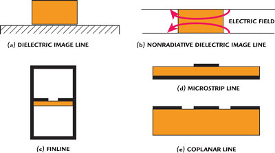
Fig.1 Cross sections of different planar and quasi-planar transmission lines.
In recent years, some effort has been made to introduce a modified version of a dielectric line. Known as the nonradiative dielectric (NRD) transmission line,16 it is where a dielectric slab is placed between two metal planes with the major component of the electric field parallel to the metal planes, as shown in Figure 1(b). Starting from metal waveguide, a planar substrate can be placed in the E-plane of a waveguide (mostly of the same dimension as the standard metal waveguide), typically called finline, as shown in Figure 1(c).17,18 The metallization on the substrate forms a slot in which the field is guided.
In this way, all circuit elements can be realized by a printed metallization pattern on the substrate, and semiconductor elements, preferably in the form of beam-lead devices, can easily be soldered, glued, or bonded onto these planar circuits, while the mechanical requirements for the waveguide channel can be greatly relaxed. Figure 2 shows a mount and substrate of a 60 GHz balanced finline mixer.18 The major advantage of this type of mixer is the inherently broadband 180° hybrid formed by the combination of finline and coplanar line where beam-lead diodes are placed (see inset of Figure 2).

Fig.2 Waveguide block and substrate of a 60 GHz balanced finline mixer.
Although several functions can be integrated into a single waveguide block,18 finline is hardly compatible with monolithic integrated circuits, and thus has not proven to be an optimal medium for mass production of mm-wave circuits. In parallel, microstrip circuit technology (see Figure 1(d)) was extended from low frequencies to the mm-wave range.19 Substrate thickness is reduced to as low as 0.1 mm, and quartz glass, alumina, or even soft (PTFE-based) substrates are used. In addition, semiconductor substrates can be employed, leading to the option of mm-wave monolithic integrated circuits (MMIC). Later, coplanar transmission line technology (see Figure 1(e)) was evaluated and applied to mm-wave circuits.
Coplanar line technology exhibits properties that make it extremely interesting for monolithic integration:
- All metallization elements are on top of the substrate; in general, no substrate thinning, no backside metallization, and no vias are necessary.
- A given characteristic impedance can be achieved by properly selecting the strip width and slot width.
In this way, both can be made very small, and the overall substrate area for a circuit can be reduced considerably, leading to a higher number of monolithically integrated circuits (chips) per wafer and therefore lower cost per chip. In the last decade, more complex arrangements have been employed using multilayer structures, combining different types of transmission lines and substrate types, together with monolithic integrated circuits to efficiently combine MMICs, passive or hybrid integrated mm-wave structures, IF and signal processing circuits as well as DC power supply distribution networks. Important developments and progress have also been made in the areas of interconnect methods like wire and flip-chip bonding or ball-grid or land-grid arrays.12,20,21 Also, the combination of a multilayer printed circuit board (FR4) with a thin microwave substrate laminated on top and integrated transition to waveguide has proven to be an effective integration technology, as will be discussed later in this article.
Devices and Circuits
In the early days, mm-wave circuits were mainly based on GaAs Gunn diodes or silicon IMPATT diodes for signal generation, and Schottky diodes for down conversion. GaAs Gunn diodes deliver some tens to a few hundreds of mW up to about 60 GHz. For higher frequencies, a harmonic mode of operation is necessary.22 At 94 GHz, IMPATT diodes can achieve a maximum CW output power of 1 W and up to about 15 W in pulsed operation.
Due to their low impedance and critical stability, however, oscillator design requires special care. Higher power levels can be achieved by power combining techniques or even tubes. Nevertheless, complex systems were designed based on these devices, e.g., the first automotive radars, a railway communication system and a coherent, dual-polarization pulse radar at 94 GHz with 8 W of output peak power and 50 ns of pulse width.3,23,24 For higher integration of receivers, first mm-wave monolithic integrated circuits on GaAs were realized based on Schottky diodes for mixers and field effect transistors (FET) for IF amplifiers,25,26 but soon the increase of operating frequencies of FETs and the development of heterostructure field effect transistors (HFET or HEMT)27,28 in the 1980s completely changed the situation.
Following on from that, amplifiers, oscillators, frequency multipliers and active downconverters were realized as monolithic integrated circuits on GaAs,29 and partly on InP, which are now available commercially from different suppliers. Furthermore, heterostructure bipolar transistors (HBT), both on GaAs and on SiGe, were developed and introduced to the market. In particular, the HBTs on silicon offer great cost reductions due to a better established and cheaper semiconductor technology for silicon;30 even complete front-ends for 77 GHz automotive radars are under development.31
Also, for some years now, CMOS circuits have reached operating frequencies in the mm-wave range,32 possibly opening up the opportunity for cheap mass production of mm-wave ICs. It must be stated, however, that the mask cost for CMOS circuits is rather high, so the price per IC can be low only for very large quantities.
Antennas
In general, many types of antennas can be employed in the mm-wave frequency range. As the size of mm-wave antennas scales with wavelength, it is possible to build electrically very large antennas (with respect to wavelength), that are, nevertheless, geometrically small. In planar arrays, tree-type or corporate feed networks are required to maintain the limited bandwidth of planar radiating elements. Consequently, feed losses in planar corporate feed networks emerge as a major problem, as can be seen from Figure 3.

Fig.3 Directivity, loss and gain for a square microstrip array with corporate feed network (assuming element distance λ, transmission line loss 0.15 dB per guide λ).
With increasing antenna size, feed losses dominate the antenna performance, and, although beam width gets smaller with increasing array size, the gain has a maximum at around 30 dB and drops for larger arrays. Series type feeding, on the other hand, typically leads to beam scanning or beam deterioration as a function of frequency even for moderate bandwidths. For large antennas, therefore, modified feed concepts should be selected.
One way is to use lower-loss transmission lines for the major part of the feed network, e.g., waveguide,33,34 which then might be fabricated by plastic injection molding,13 or to employ more standard antenna concepts with quasi-optical feeding like parabolic reflectors or lens antennas.35 To reduce the depth of such antennas, folding principles can be applied. A folded reflect array antenna36 is demonstrated in Figure 4. Twisting of the polarization and adjustment of the necessary phase angles for the lower reflector are achieved by a 45° rotation of the rectangular patches with respect to the incident electric field and specific selections of lengths and widths of the patches. This antenna has been included in the present Mercedes automotive radar (provided by Continental Automotive).

Fig.4 Cross section and photograph of present Mercedes/Continental ACC 77 GHz sensor (photo courtesy of Continental Automotive).
Systems Examples
It was not until the 1990s that mm-wave systems became a commercial success. In the communication field, the explosive growth of the mobile phone market required a corresponding extension of the underlying infrastructure. Tie lines to base stations and point-to-point links as cable replacement in urban areas were interesting applications for higher frequency systems in different frequency ranges up to 58 GHz. A 58 GHz radio link37 has already been realized using advanced and highly integrated planar integrated circuits including GaAs MMICs (see Figure 5) and a waveguide-based antenna34 fabricated using plastic injection molding and electroplating.13

Fig. 5 Front-end of 58 GHz radio link based on highly integrated planar circuits (photo courtesy of EADS).
In the automotive sector, research undertaken since the 1970s38 finally led to the first commercial automotive radar being introduced by Mercedes in 1999, soon followed by other automotive companies and suppliers. The first systems were still partly based on Gunn oscillators as the transmitter source and Schottky diodes as the first elements in the receiver. Now, the second and third generations of such systems are on the market based on more advanced technologies. While the Mercedes radar is supplied by Continental Automotive in Lindau, Germany (see Figure 4), Bosch offers a different approach based on a lens antenna.
A photograph of the sensor, an exploded view on its components and the principal four-beam performance is presented in Figure 6. The first automotive radar sensors were designed purely as systems to enhance comfort in driving—basically to supplement the automatic speed control in dense traffic situations. Their performance was not considered reliable enough for real safety applications. However, as developments have progressed, system performance has improved with respect to reliability, accuracy and field of view, so much that the systems being introduced now take over more and more operations to enhance vehicle and driver security.

Fig. 6 Exploded view and beam diagram of Bosch ACC sensor.
Further Developments
One of the major challenges in mm-wave technology—besides continuous progress in functionality and complexity—is a further reduction in production cost. This does not only concern the mm-wave circuits alone, but also the overall integration and fabrication of front-end, IF and frequency control circuitry, signal processing and bias supply using, as far as possible, well established mass production facilities. One step towards this is the use of standard multilayer printed circuit boards that contain low frequency circuits and, at the same time, serve as carriers for a thin microwave substrate laminated on the board’s surface.
Surface-mount technologies and, wherever possible, standard wire or ribbon bonding are used for the interconnects. Millimeter-wave antennas (arrays or single feeds for reflector or lens antennas; see Figure 6) may either be integrated on top of these multilayer arrangements, or transitions to standard waveguide may be integrated into such multilayer structures. The metal waveguide is placed in a normal direction to the backside of the substrate, while a small cap on the front of the circuit completes the transition (see Figure 7). Figure 8 shows the prototype of a module for 42 GHz communication realized in this configuration and includes three integrated transitions to waveguide. If necessary, even waveguide-type filters may be added as surface-mount devices.39

Fig. 7 Cross section of a transition from planar line to waveguide

Fig. 8 Photograph of 42 GHz module using PCB and SMT (photo coutesy of EADS).
An example for systems with increased complexity is an advanced, highly integrated 77 GHz automotive eight-channel radar module. Its general architecture with one transmit output and eight receiver channels is described in detail in Reference 40. At that time, the mm-wave front-end was built as a separate block and then connected to a PCB board (see Figure 9, top). A redesign has since been done using the PCB-integration approach as described above, which is shown in Figure 9 (bottom). Such a multi-channel arrangement will allow advanced beam forming techniques to enhance the field of view and the detection speed, but aims, at the same time, to be at an affordable cost.

Fig. 9 First design (top) and new PCB-based (bottom) 77 GHz radar front-end (photos courtesy of EADS).
With the availability of increasingly powerful radar sensors that were originally developed for automotive applications, other applications for such sensors have become achievable, like advanced sensing in the industrial environment or other security applications such as debris detection on airport runways.41,42 Another trend is towards systems with larger bandwidths, either for multi-gigabit/s data communication or for sensors for automotive (77 to 81 GHz) and related applications, resulting in a range resolution in the cm-range.
Another feature that is receiving increasing interest is re-configurability of mm-wave front-ends and antennas. To this end, switching or tuning elements are becoming more and more important. PIN-diode or FET-based switches are well established, but provide increased losses with increasing frequencies. MEMS switches43 have been under investigation for a number of years and have become increasingly mature. In parallel, ferroelectric materials and liquid crystal polymers are being considered in order to provide tunable components like phase shifters44 or to enable tuning of (reflect array) antenna elements for direct beam steering.45
Work still has to be done on such materials to reduce losses and to improve their thermal performance. For a number of applications like automotive sensors, system size is of major importance. Also, cut-off frequencies of semiconductor devices have far exceeded the 100 GHz mark, bringing systems at higher frequencies into reach.46 For example, an automotive sensor at 122 GHz is about 60 percent smaller than a 77 GHz sensor. Thus, in the near future, work on commercial systems will continue at frequencies above 100 GHz.
Conclusion
While the general ideas for mm-wave systems and their applications originated quite some time ago, it has taken nearly 50 years for a number of applications in this frequency range to have been proven technically and to become commercially successful. A great deal of technological progress was necessary in terms of integration techniques, interconnects and packaging, and finally cost-effective production techniques. What I have not mentioned, but what has also been of great importance, is the commercial availability of powerful electromagnetic and circuit simulators, both linear and nonlinear, and the progress in easy-to-handle and precise measurement equipment for the mm-wave range. Even today, mm-wave systems are more expensive than those at lower frequency, but additional work is under way. For one of the most promising commercial applications, the automotive area, it is believed that, similar to other electronic equipment like automatic breaking systems (ABS) or electronic stability programs (ESP), mm-wave radar sensors will move from the present luxury class system to a security system for all cars.
References
1. W. Straiton and C.W. Tolbert, “Millimeters—The New Radio Frontier,” Microwave Journal, January 1960, pp. 37–39.
2. H.M. Barlow, “Long-distance Transmission by Waveguide,” Brit. Commun. & Electronics, Vol. 6, February 1959, pp. 92–95.
3. K. Lindner and W. Wiesbeck, “35 GHz Pulse-radar Sensor Employed for a Distance Warning System in Cars (in German),” Nachrichtentechnische Zeitung, Z29, H9, September 1976, pp. 667–672.
4. J.C. Wiltse, “Millimeter-wave Technology & Applications,” Microwave Journal, August 1979, pp. 39–42.
5. C.R. Seashore and D.R. Singh, “Millimeter-wave ICs for Precision Guided Weapons,” Microwave Journal, June 1983, pp. 51–63.
6. H.H. Meinel, “Commercial Applications of Millimeter-waves: History, Present Status and Future Trends,” IEEE Transactions on Microwave Theory and Techniques, Vol. 43, July 1995, pp. 1639–1653.
7. H.J. Kuno, “Are Millimeter-wave Systems Affordable Now?,” Microwave Journal, June 1982, pp. 16–25.
8. J.C. Wiltse, “The Maturation of Millimeter-wave,” Military Technology (MILTECH), September 1984. pp. 98–109.
9. D.M. Russell, “MM-wave Snapshot Reveals Maturing Technology,” Defense Electronics, October 1984, pp. 113–115.
10. N.B. Kramer, “Must mm-waves Wait Again?,” Microwave Journal, July 1985, pp. 24–26.
11. E. Braun, “Progress in Millimeter Waves—Where is the Infrastructure?,” Defense Electronics, December 1986, pp. 77–82.
12. W. Menzel, J. Kassner and U. Goebel, “Innovative Packaging and Fabrication Concept for a 28 GHz Communication Front-End,” IEICE Transactions on Electronics-C, Japan, Special Issue on “High-Frequency/High-Speed Devices for Information and Communication Systems to Support 2K Society,” Vol. E82-C, No. 11, November 1999, pp. 2021–2028.
13. R. Dolp, W. Mayer and W. Grabherr, “Industrialization of a 58 GHz High Gain Flat Panel Antenna Design Using Injection Molding Technique,” European Microwave Conference, October 1999, pp. 13–15.
14. R.T. Davis, “Millimeter-waves: Controversy Brews Over Transmission Media,” Microwaves, March 1976, pp. 32–42.
15. R.M. Knox, “Dielectric Waveguide: A Low-cost Option for ICs,” Microwaves, March 1976, pp. 56–64.
16. T. Yoneyama and S. Nishida, “Nonradiative Dielectric Waveguide for Millimeter-wave Integrated Circuits,” IEEE Transactions on Microwave Theory and Techniques, Vol. 29, November 1981, pp. 1188–1192.
17. K. Solbach, “The Status of Printed Millimeter-wave E-plane Circuits,” IEEE Transactions on Microwave Theory and Techniques, Vol. 31, February 1983, pp. 107–21.
18. W. Menzel, “Integrated Fin-line Components for Communication, Radar and Radiometer Applications,” Infrared and Millimeter Waves, Vol. 13, Academic Press, 1985, pp. 77–121.
19. T.H. Oxley and C. Burnett, “Millimeter-wave (30 to 110 GHz) Hybrid Microstrip Technology,” Microwave Journal, March 1986, pp. 36–44; May 1986, pp. 177–185.
20. J. Heyen, T. von Kerssenbrock, A. Chernyakov, P. Heide and A.F. Jacob, “Novel LTCC/BGA Modules for Highly Integrated Millimeter-wave Transceivers,” IEEE Transactions on Microwave Theory and Techniques, Vol. 51, December 2003, pp. 2589–2596.
21. M.M. Tentzeris, “Multilayer (3D) Wireless, RF and Millimeter-wave Passives and Modules Using SOP Technology,” 2007 Topical Meeting on Silicon Monolithic Integrated Circuits in RF Systems, pp. 181–182.
22. H. Barth, “A Wideband Backsort Tunable Second Harmonic W-band Gunn Oscillator,” IEEE International Microwave Symposium 1981, pp. 334–338.
23. H. Meinel, A. Plattner and G. Reinhold, “A 40 GHz Railway Communication System,” IEEE Journal on Selected Areas in Communications, Vol. 1, September 1983, pp. 615–622.
24. H. Barth, W. Menzel, A. Plattner and J. Schroth, “A Frequency Agile 94 GHz Pulse-doppler Radar with Dual Polarization Capability,” AGARD Conference on High Resolution Air- and Space-borne Radar, Den Haag, May 1989, pp. 8–12.
25. B. Adelseck, W. Menzel and K.E. Schmegner, “A Monolithic Integrated MM-wave Frontend,” 11th Workshop on Compound Semiconductor Devices and Integrated Circuits, 04.-06.05.87, Grainau, Germany, Symposium Digest, pp. 88–90.
26. B. Adelseck, J.M. Dieudonne, K.E. Schmegner, A. Colquhoun, G. Ebert and J. Selders, “A Monolithic 94 GHz Balanced Mixer,” IEEE Microwave and Millimeter-wave Monolithic Circuits Symposium, 1990, pp. 111–114.
27. H. Moroc, “The HEMT: A Superfast Transistor,” IEEE Spectrum, February 1984, pp. 28–35.
28. U.K. Mishra, A.S. Brown, M.J. Delaney, P.T. Greiling and C.F. Krumm, “AlInAs-GaInAs HEMT for Microwave and Millimeter-wave Applications,” IEEE Transactions on Microwave Theory and Techniques, Vol. 37, September 1989, pp. 1279–1285.
29. P. Staecker, “Device Technology and Integration Techniques for Commercial mm-wave Systems,” Topical Symposium on Millimeter Waves, 7–8 July 1997, pp. 51–54.
30. T.F. Meister, et al., “High-speed SiGe HBT Technology and Applications to mm-wave Circuits,” Topical Meeting on Silicon Monolithic Integrated Circuits in RF Systems, 2004, pp. 61–64.
31. M. Hartmann, et al., “A Low-power, Low-noise Single-chip Receiver Front-end for Automotive Radar at 77 GHz in Silicon-Germanium Bipolar Technology,” IEEE Radio Frequency Integrated Circuits (RFIC) Symposium 2007, pp. 149–152.
32. W. Simburger, et al., “Silicon-based RF ICs up to 100 GHz: Research Trends and Applications,” 7th International Conference on Solid-State and Integrated Circuits Technology, 2004, Vol. 1, October 2004, pp. 12–19.
33. W. Menzel and M. Schreiner, “A 38 GHz Microstrip Array with an E-plane Waveguide Feeding Network,” European Microwave Conference 2000, Vol. III, pp. 24–27.
34. T. Sehm, A. Lehto and A.V. Räisanen, “A High-gain 58 GHz Box-horn Array Antenna with Suppressed Grating Lobes,” IEEE Transactions on Antennas and Propagation, Vol. 47, July 1999, pp. 2744–2747.
35. T. Binzer, M. Klar and V. Gross, “Development of 77 GHz Radar Lens Antennas for Automotive Applications Based on Given Requirements,” 2nd International ITG Conference on Antennas INICA ’07, March 2007, pp. 205–209.
36. W. Menzel, D. Pilz and R. Leberer, “A 77 GHz FM/CW Radar Front-end with a Low-profile, Low-loss Printed Antenna,” IEEE Transactions on Microwave Theory and Techniques, Vol. 47, December 1999, pp. 2237–2241.
37. P. Mikkonen, “Modern 60 GHz Radio Link,” European Microwave Conference 1999, pp. 83–86.
38. H.H. Meinel, “Automotive Millimeter-wave Radar History and Present Status,” European Microwave Conference 1998, pp. 619–629.
39. T.J. Müller, “SMD-type 42 GHz Waveguide Filter,” IEEE International Microwave Symposium, Vol. 2, June 2003, pp. 1089–1092.
40. W. Mayer, M. Meilchen, W. Grabherr, P. Nüchter and R. Gühl, “Eight-channel 77-GHz Front-end Module with High-performance Synthesized Signal Generator for FM-CW Sensor Applications,” IEEE Transactions on Microwave Theory and Techniques, Vol. 52, March 2004, pp. 993–1000.
41. K. Nienhaus, R. Winkel, W. Mayer, A. Gronau and W. Menzel, “An Experimental Study on Using Electronically Scanning Microwave Radar Systems on Surface Mining Machines,” IEEE RADAR Conference 2007, Boston, MA, pp. 509–512.
42. P. Feil, W. Menzel, T.P Nguyen, C. Pichot and C. Migliaccio, “Foreign Objects Debris Detection (FOD) on Airport Runways Using a Broadband 78 GHz Sensor,” accepted for presentation at the European Microwave Conference 2008, Amsterdam, The Netherlands.
43. G. Rebeiz, RF MEMS: Theory, Design and Technology, John Wiley & Sons Inc., Hoboken, NJ, 2003.
44. E.G. Erker, A.S. Nagra, Y. Liu, P. Periaswamy, T.R. Taylor, J. Speck and R.A. York, “Monolithic Ka-band Phase Shifter Using Voltage Tunable BaSrTiO3 Parallel Plate Capacitors,” IEEE Microwave and Guided Wave Letters, Vol. 10, January 2000, pp. 10–12.
45. R. Marin, A. Mössinger, J. Freese, A. Manabe and R. Jakoby, “Realization of 35 GHz Steerable Reflect Array Using Highly Anisotropic Liquid Crystal,” IEEE Antennas and Propagation Society International Symposium, July 2006, pp. 4307–4310.
46. M. Steinhauer, H. Irion, M. Schott, M. Thiel, H.O. Ruoss and W. Heinrich, “SiGe-based Circuits for Sensor Applications Beyond 100 GHz," IEEE International Microwave Symposium, June 2004, pp. 223–226.
 Wolfgang Menzel received his Dipl.-Ing. degree in electrical engineering from the Technical University of Aachen, Germany, in 1974, and his Dr.-Ing. degree from the University of Duisburg, Germany, in 1977. From 1979 to 1989, he was with the millimeter-wave department at AEG, Ulm, Germany (now EADS). From 1980 to 1985, he was head of the laboratory for Integrated Millimeter-Wave Circuits. From 1985 to 1989, he was head of the entire millimeter-wave department. During that time, his areas of interest included planar integrated circuits, planar antennas and systems in the mm-wave frequency range. In 1989, he became a full professor at the Institute of Microwave Techniques, University of Ulm, Germany. His current areas of interest include multilayer planar circuits, waveguide filters and components, antennas, mm-wave and microwave interconnects and packaging, and mm-wave application and system aspects.