
On 14 February 2002, the Federal Communications Commission (FCC) released its First Report and Order1 to permit the unlicensed use of ultra wideband (UWB) devices in the 3.1 to 10.6 GHz frequency band with an emission limit of –41 dBm/MHz. Due to the prohibition of high power amplification under the FCC Part 15 regulations, the UWB devices are restricted to operate at very low power. The announcement has attracted worldwide interest in low power UWB research and development as it opens many opportunities in short-range and high speed wireless communications, radio frequency identification (RFID), vehicular radar systems, imaging systems, short-range positioning system (geolocation) and handheld applications, etc.
To address this emerging wireless technology, IEEE 802.15 WPAN Task Group 3 (TG3a) and Task Group 4 (TG4a) are currently drafting standards specifications for short-range, high rate communications and low rate positioning systems. Proposed methods for implementing UWB solutions include time modulation UWB (TM-UWB), direct-sequence spread-spectrum impulse radio (DS-UWB), multi-band orthogonal frequency division multiplexing (MB-OFDM) and multiband-impulse (MB-I) technologies. Regardless of the type of technology employed for UWB communication, except for MB-OFDM, the fundamental type of source required is a pulsed RF source. In this article, the characteristics of sub-nanosecond rectangular pulses in the frequency domain are briefly presented. With reference to a few types of devices suitable for short pulse generation, typical impulse circuit topologies are discussed with a focus on the step recovery diode. Using shunt short-circuited transmission lines as a pulse-shaping network, the impulse can be further formed into a polycycle Gaussian pulse.
Pulse Characteristics
Commonly used signals for UWB applications are step-like pulse, impulse, rectangular pulse, monocycle and polycycle pulse. To comply with the FCC power spectral mask from 3.1 to 10.6 GHz, these signals must be shaped with some kind of filtering techniques. Therefore, it is important to understand the time response and frequency spectral content of these signals. Generation of an ultra-short pulse relies on the transition speed of a step (Ts) or the duration of the impulse (Td).2 If it is desired to fully utilize the 3.1 to 10.6 GHz frequency band, the pulse duration should be less than 100 ps. To validate the relationship of the pulse width with respect to the equivalent output spectrum, a simple experiment can be carried out. An Anritsu pulse pattern generator is used to generate two rectangular pulses with amplitude of 0.25 V referenced at 0 V, with a period of 3.2 ns, and pulse widths of 100 ps and 200 ps, respectively. The equivalent spectrum of each pulse is similar to a sinc (x) curve, as shown in Figures 1 and 2. The first null of the rectangular pulse occurs at 1/Td, which is at 10 GHz for a Td of 100 ps and at 5 GHz for a Td of 200 ps. It is also obvious that the second and third nulls of the 200 ps rectangular pulse occur at 10 and 15 GHz, respectively.

Fig. 1 Spectral content of a rectangular pulse of 100 ps duration and 3.2 ns period.

Fig. 2 Spectral content of a rectangular pulse of 200 ps duration and 3.2 ns period.
Depending on the type of application, the pulse repetition frequency (PRF) is another design consideration as it affects the output frequency content. The pulse repetition rate is the inverse of the pulse period.
The pulse with a period of 3.2 ns has a PRF of 312 MHz. For pulses with duration of 100 ps, and periods of 6.4 ns, 12.8 ns and 25.6 ns, the equivalent measured PRFs are approximately 156, 78 and 39 MHz, respectively, as shown in Figures 3, 4 and 5. The separation between adjacent spectral peaks will be narrower if the pulse period is longer. It is noticeable that the spectral peaks are very close to each other at a pulse repetition frequency of 39 MHz. Due to the lower PRF, the overall power level of the spectra is proportionally low.

Fig. 3 Spectral content of a rectangular pulse of 100 ps duration and 6.4 ns period.

Fig. 4 Spectral content of a rectangular pulse of 100 ps duration and 12.8 ns period.

Fig. 5 Spectral content of a rectangular pulse of 100 ps duration and 25.6 ns period.
Ultra-short Pulse Generation
There are many techniques and approaches for short pulse generation, which are mainly developed from UWB radar applications. A century ago, a conventional method of generating ultra-short pulses used spark gaps with arc discharges between carbon electrodes. With the evolution of technology, the variety of devices used for generating ultra-short steps or pulses has expanded to include gallium arsenide (GaAs) photoconductive switches,3–4 mercury switches, avalanche transistors, step recovery diodes (SRD), tunnel diodes and avalanche diodes, etc. Table 1 shows the typical characteristics of some of these devices.

In high power radar applications, pulse generation is usually accomplished using avalanche diodes, GaAs photoconductive switches or mercury switches. In this article, high power devices are ignored and the concentration is on low cost pulsers for low power UWB communications. The principle of ultra-short pulse generation is through charge-storage and the discharging of these devices with a trigger input signal. The avalanche effect in either a transistor or some kind of discharge/switching diode produces nonlinear characteristics. The nonlinearity results in very fast rise times for step or pulse generation. The physics of conduction and intrinsic capacitive nonlinearity in each device will not be discussed as the focus here is on UWB signal generation from a device and circuit perspective. Interested readers can refer to Reference 6 for a more comprehensive understanding of the nonlinear behaviors of the devices. Based on the best available rise time at amplitude in Table 1, it is clear that avalanche transistors, tunnel diodes and step recovery diodes are the best choices for low power ultra-short pulse generation.
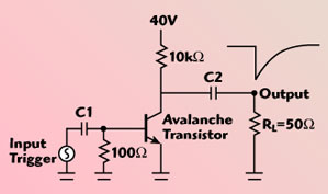
Fig. 6 Pulse generator circuit using an avalanche transistor.
Figure 6 shows a typical impulse generator circuit using an avalanche transistor. Short impulses will be generated when the trigger source excites the base of the transistor. Even though the best achievable rise time is 150 ps (as shown in Table 1), a high DC voltage is required to power up the transistor. Owing to the overheating caused by avalanching, the pulse repetition rate is limited to the kilohertz to megahertz range. Since an avalanche transistor consumes a high DC power and has a low pulse repetition rate, it is not a good choice for low power and high data rate UWB systems. A tunnel diode, which has the fastest transition time among others, is the best device to be used for step-like pulse generation. However, the disadvantage of using a tunnel diode is its low output voltage of 0.25 to 1 V for the best available rise time. The output voltage will be in tenths of a millivolt (mV) after pulse shaping. As a result, a post-amplifier is normally required to subsequently amplify the output voltage. Figure 7 shows the schematic diagram of an impulse generator circuit with a tunnel diode that produces output pulses or oscillations. The circuit with a variable operating point, having a transfer function that is defined in Lye and Joe,7 is excited by cyclical input analogue waveforms to generate ultra-short pulses.

Fig. 7 Pulse generator circuit with tunnel diode shunted to the ground.

Fig. 8 Typical configurations of pulse generator circuits using step-recovery diodes.
To achieve higher amplitude of output voltage and satisfy rapid rise time requirements, an SRD could be the most promising device for ultra-short pulse generation in low cost and low power UWB applications. SRDs are widely used as impulse generators by UWB research groups as well as in novel circuits reported in recent publications.8–11 Figure 8 shows typical impulse generator circuits with an SRD placed in series8–10 (a) to the trigger source or (b) shunt across a microstrip line.11 An input trigger source drives the series SRD that generates a step-like pulse. It is further divided to deliver two equal step-like pulses to the short-circuited stub and load. The reflected step-like pulse from the short-circuited stub, which is 180° out of phase with the incident pulse, combines with the next step-like pulse propagating toward the load to form a positive impulse at the output. For the shunt SRD, the energy is charged-stored in the series inductor during the positive half interval of the input trigger. In the negative half interval, the diode snaps off when the voltage drops below a threshold value. The conduction current falls rapidly to zero and an impulse is formed during discharging. Regardless of the placement of the SRD, the main design constraint for a UWB pulse generator is a wideband impedance matching. Poor matching of the output of the pulse generator to the load impedance will lead to a severe ringing phenomenon. To overcome this constraint, some practical approaches using impulse-shaping circuits are discussed next.
Fig. 8 IEEE 802.15.4 and Zigbee working model.
Impulse Generation Using SRD
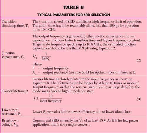
The generation of sub-nanosecond pulses is mainly governed by the snap/transition time and junction capacitance of an SRD. To achieve good performance and minimize the cost of an impulse generator, the major criterion to be considered is the SRD selection. Typical parameters of an SRD are listed in Table 2. The performance of the SRD relies on each of the parameters described in the notes. It has been shown previously that the high frequency content of a pulse is affected by the pulse width. Therefore, an SRD with very short transition time (Tt) and low junction capacitance (Cj) is required to generate a sub-nanosecond pulse. For instance, impulses with full width at half maximum (FWHM) of approximately 200 ps have been generated by using both an SRD that has a Tt of 30 ps and Cj of 0.25 pF8 or an SRD that has a Tt of 75 ps and Cj of 0.6 pF.9–10 In both cases, the pulse repetition rate reported was 10 MHz.
The most important design consideration in an impulse circuit design is to minimize the distortion caused by ringing in the output waveform. The practical solution is to improve the impedance matching between the impulse generator circuit and the pulse-shaping circuit. Techniques applied in the design of an impulse-shaping circuit include simple matching using microstrip line stubs11 to reduce the signal reflections between the circuits, the combination of a MESFET amplifier and a Schottky diode,8 or a resistive matching network and Schottky diodes for rectifying and switching.9–10
It is obvious from Table 1 that an SRD with greater rise time will have a lower breakdown voltage. A device with extremely fast transition time would have a slightly higher cost. As emerging UWB communications applications seek low cost as a goal, a novel impulse generator design technique has been reported,12 using a relatively poor and thus low cost SRD with a Tt of 150 ps and Cj of 1 pF. The pulse generator requires 0.5 V, < 100 mA of the DC supply, and an input sinusoidal or rectangular waveform trigger at 10 dBm. In fact, DC bias is an advantageous approach as it helps to reduce the required input trigger power and provides a degree of freedom for optimizing the output waveform. The circuit is capable of generating ultra-short impulses with pulse repetition rates from 10 MHz to at least 200 MHz, depending on the frequency of the input trigger. The improvement of this impulse generator’s performance is due to a simple passive impulse-matching network, which helps to achieve wideband impedance matching. The pulse width, measured using an Agilent wide-bandwidth oscilloscope, is less than 200 ps, as shown in Figures 9 and 10. Figure 11 shows the equivalent frequency content of the impulse with a PRF of 100 MHz. The cost of all components used in this prototype was less than US$0.60.

Fig. 9 Simulated and measured impulse with a PRF of 10 MHz.

Fig. 10 Simulated and measured impulse with a PRF of 100 MHz.
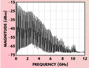
Fig. 11 Measured frequency spectrum of an impulse with a pulse width of less than 200 ps.
Pulse Shaping
The fractional bandwidth of UWB transmission systems is defined as 2(fH–fL)/ (fH+fL), where fH and fL are the highest and lowest frequencies of the UWB bandwidth, respectively. The UWB signal can be shaped to occupy only a certain bandwidth. It was reported13 that the fractional bandwidth decreases as the order of the derivative of the Gaussian pulse increases. From this point of view, the time-domain waveform for a multi-band scheme will have a higher order of derivative as compared to a single-band scheme. To comply with the FCC power spectral limit, the high order of derivative of a Gaussian pulse, or polycycle Gaussian pulse, could be a more appropriate signal because it has a bandpass frequency spectrum and a smaller fractional bandwidth. The challenge for the pulse-shaping circuit lies in converting the impulse to a polycycle Gaussian pulse. The conventional approach uses a wide-bandpass filter to truncate the spectra on a selected frequency band, which is 3.1 to 10.6 GHz in this context. UWB antennas can behave as wide-bandpass filters if properly designed. However, the design specifications for UWB antennas will be very stringent to meet the specific requirements of bandpass filtering, antenna gain and the type of polarization simultaneously. Therefore, it is recommended to include a pulse-shaping network prior to transmission.
A polycycle Gaussian pulse can be realized using multiple sections of short-circuited transmission lines, as shown in Figure 12. The impulse arriving at the first junction will split into two equal impulses to L1 and l2. The impulse propagates along L1 and is reflected back to the junction from the short-circuited stub. It combines with the next incoming impulse and forms a monocycle pulse if the time delay (length of l1) is properly optimized. Thus, a polycycle pulse can be formed from multiple reflections from the short-circuited stubs, ‘L1’ to ‘Ln’, combining with the next incoming pulse. The lengths of ‘,’ and ‘L’ have to be properly tuned to obtain a polycycle pulse with minimum distortion. Based on this principle, a monocycle Gaussian pulse has been reported8–10 using only a single short-circuited transmission line.

Fig. 12 Typical passive pulse shaping circuit.
The method explained above can be realized easily using a microstrip line but the physical dimension of the passive pulse-shaping circuit employed could be relatively large. To overcome this constraint, a novel design technique using an active pulse-shaping circuit has been reported.12 Using a 100 MHz impulse source to drive the novel active pulse-shaping circuit, which uses an amplifier,12 a Gaussian pulse with a fourth-order derivative is measured, as shown in Figure 13. Note that the measured waveform is shifted by –0.15 V for clearer distinction. Figure 14 shows the equivalent frequency spectrum of the Gaussian pulse with a fourth-order derivative. The spectrum spreads across a wide frequency band from 2.5 to 10 GHz with a PRF of 100 MHz.

Fig. 13 Simulated and measured time-domain waveform using an active pulse shaping circuit.

Fig. 14 Measured frequency spectrum of a Gaussian pulse with fourth-order derivative.
Conclusion
A sub-nanosecond pulser is a key enabling component for low power UWB applications. The characteristics of the UWB pulse should be carefully designed to fully utilize the power spectrum efficiently. Depending on how the technology is deployed, proper spectral filtering is required to comply with the FCC power spectral mask. Novel impulse generators and pulse-shaping design techniques must be further explored and developed to achieve more cost-effective, miniaturized UWB pulse sources. The measurements presented in this article were taken on the prototype developed by the author to keep abreast with the emerging technology.
Acknowledgments
The author would like to thank Anritsu Co. (Singapore) for loaning the pulse pattern generator MP1763C demonstration unit and Agilent Technologies (Singapore) for loaning the wide-bandwidth oscilloscope, Infiniium DCA 86100B, and the spectrum analyzer, E4407B (ESA-E Series), for prototype measurement.
References
1. Revision of Part 15 of the Commission’s Rule Regarding Ultra Wideband Transmission Systems, FCC 02-48, First Report and Order, Washington, DC, 22 April 2002, http://hraunfoss.fcc.gov/edocs_public/attachmatch/FCC-02-48A1.pdf.
2. J.R. Andrews, Picosecond Pulse Generator for UWB Radar, AN-9, Picosecond Pulse Labs, Boulder, CO, May 2000.
3. J.S.H. Schoenberg, J.W. Burger, J. Scott Tyo, M.D. Abdalla, M.C. Skipper and W.R. Buchwald, “Ultra Wideband Source Using Gallium Arsenide Photoconductive Semiconductor Switches,” IEEE Transactions on Plasma Science, Vol. 25, No. 2, April 1997, pp. 327–334.
4. M. Fanbao, Z. Chuanming, Y. Zhoubing, J. Bingquan, W. Wentao and M. Hongge, “UWB Pulse Generation and Radiation Using a Photoconductive Switching in GaAS,” IEEE 18th International Symposium on Discharges and Electrical Insulation in Vacuum, Eindhoven, The Netherlands, May 1998, pp. 785–787.
5. T.W. Barrett, “History of Ultra Wideband (UWB) Radar & Communications: Pioneers and Innovators,” Progress in Electromagnetics Symposium 2000, Cambridge, MA, July 2000, p. 9.
6. S.A. Maas, Nonlinear Microwave and RF Circuits, Second Edition, Artech House Inc., Norwood, MA, 2003.
7. K.M. Lye and J. Joe, “Method and Apparatus for Generating Pulses from Analog Waveforms,” United States Patent Application Publication, US2002196065, December 26, 2002.
8. J.S. Lee and C. Nguyen, “Novel Low Cost Ultra Wideband, Ultra-short-pulse Transmitter with MESFET Impulse-shaping Circuitry for Reduced Distortion and Improved Pulse Repetition Rate,” IEEE Microwave Wireless and Components Letters, Vol. 11, May 2001, pp. 208–210.
9. J.S. Lee, C. Nguyen and T. Scullion, “New Uniplanar Sub-nanosecond Monocycle Pulse Generator and Transformer for Time-domain Microwave Applications,” IEEE Transactions on Microwave Theory and Techniques, Vol. 49, No. 6, June 2001, pp. 1126–1129.
10. J.W. Han and C. Nguyen, “A New Ultra Wideband, Ultra-short Monocycle Pulse Generator with Reduced Ringing,” IEEE Microwave and Wireless Components Letters, Vol. 12, No. 6, June 2002, pp. 206–208.
11. K. Madani, et al., “A 20 GHz Microwave Sampler,” IEEE Transactions on Microwave Theory and Techniques, Vol. 40, No. 10, October 1992, pp. 1960–1963.
12. Y.W. Yeap and C.L. Law, “UWB Impulse and Polycycle Pulse Generation with ON-OFF Keying Modulation,” United States Provisional Patent Application, July 16, 2004.
13. M. Welborn and J. McCorkle, “The Importance of Fractional Bandwidth in Ultra Wideband Pulse Design,” IEEE International Conference on Communications Digest, Vol. 2, 2002, pp. 753–757.
Yeap Yean Wei received his B.Eng degree in communications and electronics engineering from Northumbria University, UK, in 2002. He is currently working as an associate consultant in the Network Technologies Group, Infocomm Development Authority of Singapore. His job responsibilities include identifying, tracking and exploring emerging technologies in wireless network domains.