

Recent developments in most consumer electronic products is toward miniaturization. The technology of integrated circuits is widely applied in the field of communication baseband modules and radio frequency modules to make communication products smaller in size. On the contrary, the technology of integrated circuits is difficult to use to design a compact antenna. Therefore, the design of compact antennas becomes a critical technique to reduce the size of communication products.
A Planar Inverted F Antenna (PIFA) is a major structure in compact antennas. There are detailed discussions in the literature.1–3 The PIFA antenna is also usually used in the design of dual-band4–6 and diversity antennas.7 The outstanding feature of the antenna is its &lamda;/4 resonant length. The advantage over monopole antennas and microstrip antennas is planar geometry and no dielectric loss, respectively. The design method of using a capacitive load to minimize the PIFA antenna has been discussed.1
The goal of this article is to use an alternative method to design the antenna that performs as well as a PIFA antenna. Figure 1 shows the structure of the antenna. The feeding position is adjusted such that the total length of the radiator and ground forms the &lamda;/2 length; the phase of the current on the radiator conductor will then be consistent. The length of the radiator on the antenna is &lamda;/4, the same as the PIFA antenna. This article also discusses the influence of antenna height and width to the resonant frequency, and shows that the increasing width and height of the antenna lowers its resonant frequency. In order to minimize the antenna size, the applicable geometry is etched on the radiator or ground that will induce the slow-wave effect on the antenna. Figure 2 illustrates the structure of the etching geometry. The etching geometry increases the equivalent inductance and capacitance that will decrease phase velocity on the antenna to minimize antenna size.
Antenna Module and Slow-wave Effect Application
Antenna Configuration
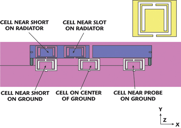
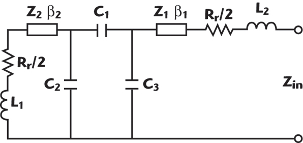
As shown in Figure 3, the antenna transmission module is divided into two segments. One is the upper radiator composed of two conductors with one-eighth wavelength. The other is the lower ground with a quarter-wavelength. The feeding port uses the coaxial feed. The position of the feeding port can be placed on one of the two ends. If one side on the antenna is the feed position, the other side is the short to ground. Figure 4 illustrates the equivalent transmission line model. The slot on the upper conductor and between the two upper conductors as well as ground are modeled as the equivalent capacitors C1, C2 and C3, respectively. The short-pin end and the feeding port end are modeled as the radiation resistance R1/2 in series with the equivalent inductor L1 and radiation resistance R1/2 in series with the equivalent inductor L2, respectively. The radiation resistance and equivalent inductor are produced by the upper radiator, short pin and feeding port. The radiation resistance can transfer the energy to propagate in space when resonance occurs. In this antenna structure, the lower ground provides the phase delay β2 &lamda; l/8 and the radiator conductors provide the phase delay β1 x &lamda;/8. When the length of each conductor on the upper radiator and ground plane is one-eighth wavelength and quarter-wavelength, respectively, the phase of current on the radiator is in phase to produce the resonant phenomenon. When the resonant frequency is at 2.1 GHz, L1 = L2 = 18.5 mm, Lg = 40 mm and h = 6 mm.
An Application of the Slow-wave Effect to Minimize Antenna Size
The purpose of slow wave is to slow down the propagation phase velocity. In this article, the antenna design increases the equivalent inductance and capacitance for antenna resonance. The relationship among phase velocity, capacitance and inductance is

where
vp=phase velocity
L=equivalent inductance
C=equivalent capacitance
Increasing the inductance and capacitance can decrease phase velocity. The method of increasing inductance and capacitance is to etch applicable geometries on the antenna conductor, which is shown in Figure 4. The etched portion and thin conductor portion on the geometry increases the parallel capacitance effect as well as the series inductance effect, respectively. Therefore, it will decrease phase velocity to minimize the antenna size. The relationship of phase velocity and wavelength is

where
f= resonant frequency
λ = resonant wavelength
At the same resonant frequency, decreasing phase velocity can reduce the resonant wavelength and antenna length.
Results and Discussion

Influence of the Slow-wave Effect on the Antenna
Figure 5 shows how etching geometric figures on the conductor surface induces phase delay that will affect resonant frequency. There are two situations. The thin line shows the case without etching any geometric pattern on the conductor. The phase velocity is approximately 5.1 x 10⁶ m/s and is almost independent of frequency. The blue line shows the case with etching the geometric pattern on the antenna. The geometric pattern is shown in Figure 2. The phase velocity is approximately 4.1 x 10⁶ m/s under 4 GHz showing 20 percent reduction compared to the case without the etched structure on the conductor. The phase velocity rises above 4 GHz. At 4.2 to 4.7 GHz, the phase velocity is higher than without the etched geometric pattern. Hence, the etched geometry can only be used to design a compact antenna for less than 4 GHz.
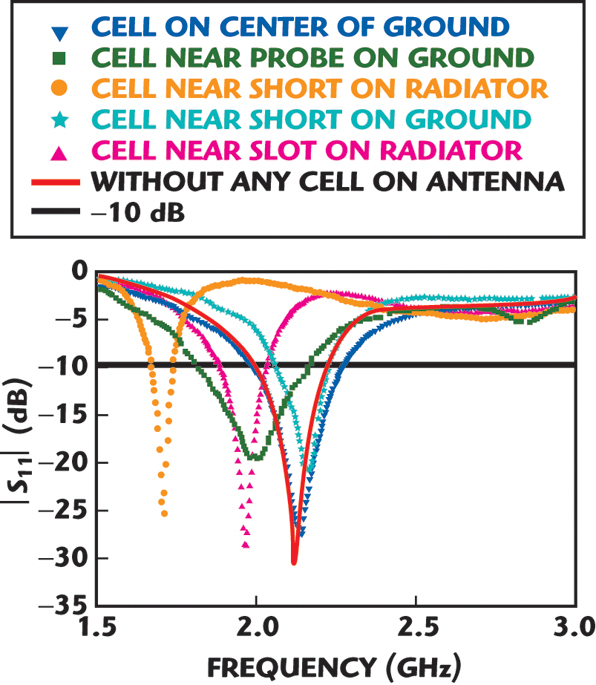
Figure 6 shows the measured return loss using a HP8720C. The affect on resonant frequency by different etching positions with the same height, length and width of the antenna will now be discussed. The reference line is without an etched pattern on that antenna. The antenna size with h = 6 mm, W = 8 mm and L1 = L2 = 18.5 mm has a resonant frequency of about 2.1 GHz. The results shown in Figure 6 indicate that etching the geometry on the radiator provides the slow-wave effect more than etching the geometry on the ground, and etching the geometry on the near short provides more effect of the slow wave because the current distribution on the antenna conductor is not uniform and near the short of the antenna provides larger current distribution; hence, the etching geometry near the short conductor of the antenna can obtain more of a slow-wave effect. Etching the geometric pattern on the ground cannot increase the effect of the slow wave because there is a larger area on the ground that causes a smaller current to flow to the antenna resonant route, thereby inducing a smaller equivalent capacitance and inductance.
The Influence of Antenna Size
Figure 7 illustrates how antenna size influences resonant frequency when the antenna size is set to h = 6 mm, L1 = L2 = 18.5 mm and different widths of W = 13 mm, 8 mm or 5 mm, respectively. Increasing the width of the antenna results in a lower resonant frequency. Increasing radiator width can increase the capacitance effect that decreases phase velocity. At the same radiator length, adjusting the width of the antenna will vary the resonant frequency. According to the results, the height of the antenna can affect resonant frequency. At the same antenna length, reducing antenna height can increase the antenna resonant frequency. According to the analysis, etching applicable geometries on the antenna or increasing width and height can achieve a lower resonant frequency because etching a geometric pattern on the antenna and increasing the width of the antenna can increase equivalent capacitance and inductance.
Results for Antenna Pattern and Gain
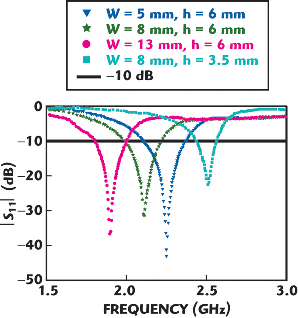
Table 1 lists the gains of all of the antennas. The upper section is classified according to the position of the etched pattern on the radiator. The gains of the first two antennas in the upper section are 2.93 and 2.10 dBi, the former with the etched pattern near the slit on the radiator, the latter with the etched pattern near the short pin on the ground. The gains of the antennas from the third to the fifth graph on the upper section are 2, 3 and 2.37 dBi for the etched pattern on the ground close to the feed, the center on the ground and the ground near the short pin, respectively. The maximum gain of the antenna is found by etching on the center on the ground. The lower section is classified according to the different widths and heights. The gains of the antennas in the lower section are 2.9, 3.41, 1.57 and 2.6 dBi with the width of radiator 5, 8, 13 and 8 mm and height of radiator 6, 6, 6 and 3.5 mm, respectively. The maximum gain of the antenna is found with the width and height of the antenna at 8 and 6 mm, respectively. Figure 8 plots the radiation patterns in sequence, the same as in Table 1. The asymmetry of the antenna radiation pattern is due to the single-end feed. Compared with the antenna without etching, the cross-polarization of the H-plane will increase by about 10 dB due to the etching structure on the antenna destroying the direction of the current on the conductor. Therefore, with the cross-polarization increased, the influence of the difference between co-polarization and cross-polarization of 10 dBi is not very large. As far as co-polarization is concerned, etching will not affect the magnitude of the radiation pattern. Changing the width and height of the antenna and etching structure could be used as methods to reduce the dimensions of the antenna.

Conclusion
A novel compact planar double inverted L antenna (PDILA) has been designed and fabricated; the length of the antenna is designed for a quarter-wavelength. The design for feeding, which is different from the conventional PIFA, is an innovative concept designed for a planar or concealed antenna. Due to no dielectric loss, this method can be used for higher frequency by modifying the width. If the applicable geometric structure is etched on the proper position of the antenna, the slow-wave effect can be measured. Moreover, etching in the position with the larger current density provides additional slow-wave effect. The effect of the slow wave will lower the resonant frequency, and hence reduce the length of the antenna. Putting the slow-wave structure on the antenna and increasing the width of the radiator are alternatives to reduce the antenna’s dimensions.

Acknowledgment
This work was sponsored by the National Science Council under contract number NSC 95-2221-E-024-025.
References
1. C.R. Rowell and R.D. Murch, “A Capacitively Loaded PIFA for Compact Mobile Telephone Handsets,” IEEE Transactions on Antennas and Propagation, Vol. 45, No. 5, May 1997.
2. K.L. Virga and Y. Rahmat-Samii, “Low-profile Enhanced-bandwidth PIFA Antennas for Wireless Communications Packaging,” IEEE Transactions on Microwave Theory and Techniques, Vol. 45, No. 10, October 1997.
3. P.K. Panayi, M.O. Al-Nuaimi and I.P. Ivrissimtzis, “Tuning Techniques for a Planar Inverted-F Antenna,” Electronics Letters, Vol. 37, No. 16, August 2001.
4. N.C. Karmakar, “Shorting Strap Tunable Single Feed Dual-band Stacked Patch PIFA,” Antennas and Wireless Propagation Letters, Vol. 2, No. 2, 2003.
5. N.C. Karmakar, “Shorting Strap Tunable Dual-band Stacked PIFA,” IEEE Antennas and Propagation Society International Symposium, Vol. 3, June 22–27, 2003.
6. F.R. Hsiao, W.S. Chen and K.L. Wong, “Dual-frequency PIFA with a Rolled Radiating Arm for GSM/DCS Operation,” IEEE Antennas and Propagation Society International Symposium, Vol. 3, June 22–27, 2003.
7. K.L. Wong, A.C. Chen and Y.L. Kuo, “Diversity Metal-plate Planar Inverted-F Antenna for WLAN Operation,” Electronics Letters, Vol. 39, No. 7, April 2003.
8. C. Caloz and T. Itoh, “Multilayer and Anisotropic Planar Compact PBG Structures for Microstrip Applications,” IEEE Transactions on Microwave Theory and Techniques, Vol. 50, No. 9, September 2002.