
UWB communication systems have recently attracted tremendous attention for industry, media and academic applications. The UWB system is a new wireless technology capable of transmitting data over a wide frequency range with low power consumption and high data rates.1,2 In order to develop UWB communication ICs with reasonable cost for consumer electronics, the integration of transceiver and receiver sub-circuits dominated the total chip size and fabrication cost. Based on previous studies, the UWB low noise amplifier, switch, and power amplifier can be designed and integrated using sub-micron Si RFCMOS or SiGe BiCMOS technologies.3,4 However, a low switch insertion loss and a small LNA noise figure in a UWB module were difficult to obtain in the Si RFCMOS or SiGe BiCMOS processes simultaneously. Therefore, a low insertion loss and low harmonic InGaP/InGaAs PHEMT switch was proposed to meet the industry criteria for a wideband switch.5
In this regard, an InGaP/InGaAs enhancement-mode PHEMT was first used and demonstrated on a UWB low noise amplifier. This process can easily be integrated with a depletion-mode InGaP/InGaAs PHEMT switch using an InGaP/InGaAs E/D-mode process.6 In the PHEMT process, the InGaP/InGaAs E-mode PHEMT includes excellent etching selectivity between the InGaP and the GaAs, which increases the device manufacturability. The high-energy bandgap of the InGaP Schottky layer results in low microwave noise and reduces the Gunn oscillation effects.7 In addition, InGaP does not form DX-centers and causes less deep-level defects, which has great potential to improve the reliability of the PHEMTs. This article describes the design and implementation of a MMIC for a 3 to 5 GHz UWB LNA using an InGaP E-mode PHEMT technology. The 3 to 5 GHz UWB LNA exhibits a 15 to 19 dB gain with 3.5 dB of average noise figure with 63 mW DC power consumption. The chip size is 1 mm2.

Device Structure, Fabrication and Performance
Figure 1 shows the epitaxial structure of the In0.5Ga0.5P/In0.24Ga0.76As E-mode PHEMTs. Two Si planar δ-doping layers are placed on either side of the InGaAs undoped channel layer with an AlGaAs spacer layer for high transconductance consideration. An undoped 100 Å InGaP Schottky layer was grown on an intrinsic GaAs layer to form a Schottky barrier. Finally, two n+–GaAs cap layers were grown to improve the ohmic contact resistivities. The designed structure demonstrated a sheet charge density of 2.2 x 1012 cm–2 together with a Hall mobility of 6120 cm2/V-sec at 300 K after removing the n+–GaAs cap layers. In the device fabrication, ohmic contacts of Au/Ge/Ni/Au metals were deposited by e-beam evaporation and patterned by a conventional lift-off process. An ion-implant isolation technology was applied for mesa isolation to avoid sidewall gate leakage current. After a highly-selective succinic acid gate recess process,6 0.5 μm long Pt/Ti/Au-gates (40 Å/500 Å/4000 Å) were deposited by a lift-off process. Prior to the deposition of the 1000 Å-thick SiNx passivation layer, the wafer was subjected to an O2 plasma treatment to clean it. Pt gate diffusion into the InGaP Schottky layer of the device was achieved during the SiNx deposition at 250°C.
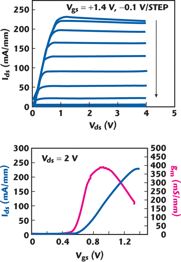
The typical drain-to-source current (Ids) versus drain-to-source voltage (Vds) and the transconductance (Vgs) characteristics of the fabricated InGaP/InGaAs E-mode PHEMT are shown in Figure 2. As can be seen, the device can be operated with gate voltages up to 1.4 V, which corresponds to a Ids of 230 mA/mm when the drain voltage is 3 V, owing to the high Schottky barrier (0.86 eV) of metal-InGaP contact and large ΔEc (0.4 eV) between the InGaP and InGaAs.8 The drain-to-source leakage current at Vds =; 2 V and Vgs = 0 V is less than 0.2 μA/mm. A low drain-to-source steady-state leakage current is beneficial for suppressing the device power consumption and signal loss, particularly at low bias conditions. The Vgs dependence of transconductance (gm) and Ids at Vds = 2 V are also shown. The threshold voltage (Vth) is 0.34 V (defined as Ids = 1 mA/mm) and the maximum Ids and gm are 235 mA/mm and 390 mS/mm, respectively. Based on a previous study, the InGaP/InGaAs E-mode PHEMT demonstrated a 0.611 dB minimum noise figure at 3 to 5 GHz operation; this range is 1.2 to 1.8 dB for the AlGaAs/InGaAs devices.9 Therefore, the InGaP/InGaAs E-mode PHEMT really offers a high potential for UWB LNA applications, owing to its low power consumption and small noise figure.

The Design of the Resistive Feedback UWB LNA
The proposed UWB LNA was fabricated using a WIN Semiconductor Enhancement/Depletion-mode PHEMT process, which has 0.5 μm gate length with a current-gain cut-off frequency (fT) of 32 GHz and a power-gain cut-off frequency (fmax) of 85 GHz. Figure 3 shows the proposed LNA topology and a microphotograph of the die of the InGaP E-mode PHEMT LNA. R1 was added as a shunt-feedback element to the conventional common-source topology. C2 is used for the AC coupling and two terminals DC isolation. For the small-signal equivalent circuit of the first stage, a Miller feedback resistance can be represented by R1 and the open loop voltage gain (AV) of the first stage of LNA [R1M = R1/(1-AV)]. For this resistive shunt-feedback topology, the proper R1M gathered the S11 values within the passband closer to the center of the Smith chart, resulting in wideband input matching. The feedback resistor also provided its conventional roles of flattening the gain over a wider bandwidth of frequencies with smaller noise figure degradation and stabilized the circuit.10 Another benefit of a proper feedback resistor R1 is to control the Q-factor of the resonating narrowband LNA circuit, which is approximately given as

R1 is 0.4 kΩ in this proposed LNA, which was realized by a mesa resistor (200 Ω/sq) to achieve a proper Q-factor for wideband matching consideration. The die size is 1 mm2.

Circuit Measurement Results
The InGaP/InGaAs PHEMT LNA for UWB applications was measured using on-wafer testing. The transistor gate dimensions of E-mode PHEMT (M1 and M2) are both 0.5 x 150 μm. As to the DC power consumption, the drain current of the input stage and the output stage are 7 and 14 mA, respectively. The gate biases for the two stages were adjusted to reach a compromise between noise figure and gm characteristics. The gate bias voltage is +0.75 V and the drain bias voltage is 3 V for the input stage, and +0.85 V and 3 V for the output stage. By using an enhancement-mode design of the active devices, the negative bias circuit can be avoided, which is a major drawback of the conventional depletion-mode PHEMT related MMICs. The measured power gain, the input/output return loss and the noise figure are shown in Figure 4. The measured input return loss (S11) and output return loss (S22) are both higher than 10.0 dB over the 3 to 5 GHz range. The flat and high S11 is obtained, due to the resistive feedback topology.
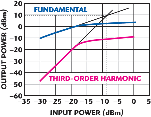
The maximum power gain (S21) is higher than 15 dB and the 3 dB bandwidth covers the 3 to 5 GHz range. The measured NF shows a minimum value of 3.4 dB at 4 GHz and stays at less than 3.6 dB up to 5 GHz, but rises up to 4 dB at 7.5 GHz. Compared to the simulation results using the self-defined Angelov model,11 the slight increase in NF over the 3 to 5 GHz range is caused by the lower power gain at these frequencies. The trend of NF between the simulation and measurements is similar. The third-order inter-modulation (IM3) product, obtained from the device output spectra versus the input power, is an important index of the device dynamic range. A two-tone evaluation was performed at frequencies of 3 and 3.001 GHz, as shown in Figure 5. A third-order input intercept point (IIP3) of –8.5 dBm and a third-order output intercept point (OIP3) of 9.7 dBm were obtained. Table 1 summarizes the comparison of recently published LNAs for UWB applications. It includes different topologies for broadband amplifiers. Although the power consumption of the proposed LNA is higher than for the other studies, the superior noise performance of this technology still offers a high potential for UWB LNA applications.
Conclusion
In this article, a low noise UWB LNA was demonstrated using InGaP/InGaAs E-mode PHEMT technology for the first time. With a resistive shunt-feedback topology, the proper R1M concentrated the S11 values in the passband closer to the center of the Smith chart, resulting in a wideband input matching. The E-mode InGaP Schottky layer design not only provides a small microwave noise, but also permits the use of a positive biasing voltage supply compared to the traditional AlGaAs Schottky layer design, which uses a negative voltage supply. The proposed E-mode InGaP/InGaAs PHEMT LNA achieved a power gain of 15 dB with a total DC power consumption of 63 mW. The measured noise figure was less than 3.6 dB from 3 to 5 GHz. Compared with the recently published broadband LNAs, the proposed E-mode InGaP/InGaAs PHEMT LNA provides a practical low noise and high gain solution for UWB applications.
Acknowledgment
The authors are grateful to the National Chip Implementation Center (CIC) for noise figure measurements and WIN Semiconductor Corp. for circuit fabrication. This work is financially supported by the National Science Council, ROC (NSC 95-2221-E-182 -058).
References
1. D. Porcino and W. Hirt, “Ultra-wideband Radio Technology Potential and Challenges Ahead,” IEEE Communication Magazine, Vol. 4, No. 7, July 2003, pp. 66–74.
2. A. Bevilacqua and A.M. Niknejad, “An Ultra-wideband CMOS Low-noise Amplifier for 3.1 to 10.6 GHz Wireless Receivers,” IEEE Journal of Solid-State Circuits, Vol. 39, No. 12, December 2004, pp. 2259–2268.
3. Y. Jin and C. Nguyen, “A 0.25 mm CMOS T/R Switch for UWB Wireless Communications,” IEEE Microwave Wireless Components Letters, Vol. 15, No. 8, August 2005, pp. 502–504
4. N. Shiramizu, T. Masuda, M. Tanabe and K. Washio, “A 3 to 10 GHz Bandwidth Low-noise and Low-power Amplifier for Full-band UWB Communications in 0.25 mm SiGe BiCMOS Technology,” 2005 IEEE Radio Frequency Integrated Circuits Symposium Digest, pp. 39–42.
5. H.C. Chiu, Y.C. Chiang and C.S. Wu, “A Low Insertion Loss Switch Using Ordering InGaP/AlGaAs/InGaAs PHEMT Technology,” Solid-State Electronics, Vol. 49, 2005, pp. 1391–1395.
6. H.C. Chiu, C.S. Cheng and Y.J. Shih, “High Uniformity Enhancement- and Depletion-mode InGaP/InGaAs PHEMTs Using Selective Succinic Acid Gate Recess Process,” Semiconductor Science and Technology, Vol. 21, 2006, pp. 55–99.
7. H.K. Huang, Y.H. Wang, C.L. Wu, J.C. Wang and C.S. Chang, “Super Low Noise InGaP Gated PHEMT,” IEEE Electron Device Letters, Vol. 23, No. 2, February 2002, pp. 70–72.
8. T.J. Miller, G.B. Backes and M.I. Nathan, “Schottky Barrier Height Modification on n- and p-type GaInP with Thin Interfacial Si,” Journal of Applied Physics, Vol. 76, 1994, pp. 7931–7934.
9. H.C. Chiu and C.S. Cheng, “Microwave Performance of (Al0.3Ga0.7)0.5In0.5P, In0.5Ga0.5P, Al0.28Ga0.72 As Enhancement-mode Pseudomorphic HEMT with Succinic Acid Gate Recess Process,” Journal of the Electrochemical Society, 2006, Vol. 153, 2006, pp. 897–900.
10. C.W. Kim, M.S. Kang, P.T. Anh, H.T. Kim and S.G. Lee, “An Ultra-wideband CMOS Low Noise Amplifier for 3 to 5 GHz UWB System,” IEEE Journal of Solid-State Circuits, Vol. 40, No. 2, February 2005, pp. 544–547.
11. C.S. Cheng, Y.J. Shih and H.C. Chiu, “A Modified Angelov Model for InGaP/InGaAs Enhancement- and Depletion-mode PHEMTs Using Symbolic Defined Device Technology,” Solid-State Electronics, Vol. 50, 2006, pp. 254–258.
12. F. Zhang and P. Kinget, “Low Power Programmable-gain CMOS Distributed LNA for Ultra-wideband Applications,” 2005 IEEE VLSI Symposium Digest, pp. 78–81.
13 M.D. Tsai and H. Wang, “A 5.4 mW LNA Using 0.35-μm SiGe BiCMOS Technology for 3.1 to 10.6 GHz UWB Wireless Receivers,” 2005 IEEE RFIC Symposium Digest, pp. 335–338.
Sheen-Chin Chiu received his BS and PhD degrees in electrical engineering from National Central University, Chungli, Taiwan, in 1998 and 2003, respectively. After receiving his PhD, he joined WIN Semiconductor Corp., Tao Yuan, Taiwan, where he was engaged in the research and development of 6-inch GaAs PHEMTs and related integrated circuits. In June 2004, he joined the faculty of Chang Gung University and began work on microwave, millimeter-wave integrated circuits, GaAs and GaN FETs fabrication and modeling.
Chia-Shih Chengreceived his BS degree in electrical engineering from Tatung University, Taipei, Taiwan, ROC, in 2004, and his MS degree in electronics engineering from Chang Gung University, Tao Yuan, Taiwan, in 2006. He is currently working toward his PhD degree at the Graduate Institute of Electronics Engineering, Chang Gung University. His research interests include RF device modeling, microwave and millimeter-wave circuit design.
Chein-Cheng Wei received his BS degree in electrical engineering from Chinese Culture University, Taipei, Taiwan, ROC, in 2002, and his MS degree in electronic engineering from Chang Gung University, Tao Yuan, Taiwan, ROC, in 2004. He is currently working toward his PhD degree in electronic engineering at Chang Gung University. His research interests include RF CMOS large-signal device modeling, RF measurement, ultra-wideband integrated circuits and millimeter-wave integrated circuits.
Yuan-Jui Shih received his BS degree in electrical engineering from Chinese Culture University, Taipei, Taiwan, ROC, in 2004, and his MS degree in electronics engineering from Chang Gung University, Tao Yuan, Taiwan, ROC, in 2006. His research interests include RF device modeling and microwave circuit design.
Shao-Wei Lin received his MS degree in electrical engineering from Chang Gung University, Tao Yuan, Taiwan, ROC, in 2007. He is currently pursuing his PhD degree at the same university. His research interests include RF devices.
Feng-Tso Chien received his BS, MS and PhD degrees in electrical engineering from National Central University, Chung-Li, Taiwan, ROC, in 1994, 1996 and 2000, respectively. He joined the department of electrical engineering at Fen-Chia University, Taichung, Taiwan, as a faculty member in 2002. His current research interests include submicron technology, III-V microwave and millimeter-wave devices, power MOSFETs and optoelectronic devices and integrated circuits.