
Phase noise is becoming generally recognized (and accepted) as a critical performance parameter in higher performing test, radar and communication systems. However, additive phase noise is not typically measured on amplifiers, frequency dividers or frequency multipliers due to the perceived difficulty of the measurement and the prohibitive cost of available phase noise measurement systems.
Contrary to popular belief, accurate additive phase noise measurements are straight-forward. Phase noise is typically considered an esoteric measurement, which many engineers and technicians would rather not have to make. This article removes the mystery from additive phase noise measurements and simplifies some of the techniques. Some knowledge of trigonometry is all that is really needed to understand additive phase noise measurements. This article demonstrates how to make valid residual phase noise measurements with a good synthesizer, low noise baseband amplifier and an audio card.
Residual or Additive Phase Noise Measurement Fundamentals
Additive phase noise, also referred to as residual phase noise, is the self phase noise of a component that adds to an existing signal as the signal passes through it. It is additive linearly, not in decibels, which would be multiplicative. The term residual phase noise is used interchangeably with additive phase noise and is in reference to the original phase noise measurement of components. The measurement system inherently subtracts out the source noise in the test system, which leaves the phase noise of the DUT, or residual phase noise, as the remainder of what is being measured. Additive phase noise is a more apt description of the noise within the system being used, rather than reference to the measurement system.
Why is additive phase noise important? Following are two examples, the first being the most obvious.
Example One
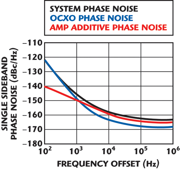
Consider a system that begins with a very low noise oven-controlled crystal oscillator (OCXO). A significant amount of work is done by the manufacturer to select appropriate internal components that add very little flicker noise to the signal. GaAs amplifiers tend to have a high flicker noise corner, a property on all amplifiers, than do silicon-based amplifiers. If a GaAs amplifier is used to amplify a very clean OCXO, it will likely degrade the phase noise in the 10 kHz region and possibly further out, depending on the signal-to-noise ratio of the amplifier operating under large signal. Equation 1 shows mathematically how the phase noise of the OCXO and amplifier, in dBc/Hz, add together

Figure 1 is a graphical representation of Equation 1, where combining the noise of a good OCXO (in blue) and that of a marginal amplifier (in red) will cause degradations in the overall phase noise of the system (in black). At the point where the phase noises of the OCXO and amplifiers are equal and identical, at 1.5 kHz, the overall noise is exactly 3 dB higher.
Example Two
This example is less obvious. Most will agree that noise figure (besides gain and P–1dB) is one of the most common specifications for an amplifier. This number does not fully represent the true added noise of an amplifier under anything but small-signal conditions and is an average for noise in carrier offset frequencies within a 4 MHz bandwidth. If one wants to measure the added noise of an amplifier when it is near compression, deep in compression, or when using a noisy power supply, the noise figure will not disclose any information that is useful under these scenarios. Additionally, the noise figure does not disclose any information about noise close to the carrier that may be important in some system. It can also be argued that additive phase noise measurements are indeed a good measurement for large-signal noise figure.
Additive Phase Noise Related to Noise Figure
Additive phase noise is directly related to noise figure under small-signal conditions. Under large-signal conditions, additive phase noise may aptly define large-signal noise figure. The traditional noise figure is an average of the additive phase noise under a very particular small-signal condition. Noise figure is defined as the degradation of the signal-to-noise ratio (SNR) at the input to the SNR at the output of a two-port device. A low noise amplifier may add less than 1 dB in a typical noise figure measurement and a standard gain block may exhibit over 5 dB. When taken out of small signal, but with an output power still near the P–1dB point, other aspects of the amplifier start to become dominant and the noise figure measurement may no longer be valid. Flicker noise, shot noise and power supply noise may contribute a more significant amount of noise to the system than the noise figure may suggest. Some amplifiers exhibit marginally more noise in compression than at small signal, while others will demonstrate heavy degradations. Only an additive phase noise measurement can identify these sources of noise.
Noise figure and phase noise measurements (at relatively small signal) relate to each other in the following way: The measured additive phase noise, fm of an amplifier at some offset frequency (fm), is related to the noise figure by the thermal noise floor (Nthermal) and the amount of input power (Pin). This relationship has been presented by A. Hati, et al.1
The thermal noise floor of a 50 ω system, denoted as Nthermal, at room temperature, is –174 dBm, which includes both amplitude and phase noise. Amplitude and phase noise each contribute to half the power of the thermal noise and are assumed to be uncorrelated, therefore leaving both the phase and amplitude of the thermal noise floor to be separately defined at –177 dBm. The value for Nthermal is then –177 dBm.
The SNR of a signal is defined as Nthermal – Pin, where Pin is the signal power in dBm. The noise figure (NF) is the reduction of the signal-to-noise ratio of a two-port device. The measured phase noise is related to the thermal noise floor, input power and noise figure by the following relation:

where
fm=measured additive phase noise at frequency offset fm
Nthermal=thermal noise floor (–177 dBm)
Pin=input power of the amplifier
NF=noise figure of the amplifier
This equation shows that the signal-to-noise ratio (Nthermal – Pin) is reduced by the noise figure resulting in the measured additive phase noise. This equation can be used to calculate the noise figure, given the measured additive phase noise and power input. The additive phase noise measurement can be used to calculate the noise figure of a device within the uncertainty of the measurement. More importantly, the additive phase noise measurement can give meaningful data on the true signal-to-noise ratio for an amplifier at large signal under real world conditions.

Figure 2 is an example of an additive phase noise measurement at a carrier of 100 MHz. The measured phase noise is –158 dBc/Hz at 10 kHz offset and the flicker corner of the device can be seen as the 10 dB per decade increase in noise, beginning at approximately 1 kHz. The input power of this amplifier was measured to be –15 dBm. Substituting the measured values for phase noise and input power into Equation 2, the noise figure is calculated to be 4 dB, exactly where this amplifier is specified to be.
How to Make Additive Phase Noise Measurements
All additive phase noise measurements start from the same basic principle. A component is driven by a sinusoidal signal source, and then the noise contributed by the signal source is cancelled out, leaving the noise contributed by the DUT. When measuring phase noise, there are two categories for two-port devices: devices that do not change the frequency and devices that do.
Amplifiers and Non-frequency Translating Devices
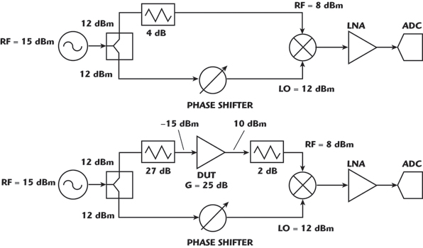
Figure 3 shows the block diagram of the additive phase noise measurement set up used to measure the sample amplifier for both small-signal and large-signal noise figure. The top diagram is to measure the noise floor of the system under the same conditions as the DUT is being measured. The difference between measuring small signal and large signal is in setting the attenuators appropriately. The set-up begins with a very clean signal source, in this case, at 100 MHz.
Using a high performance synthesizer, known to demonstrate ultra-low phase noise, is most beneficial for making these measurements accurately. The reason is that while the noise contributed by the source is theoretically cancelled, the phase detector has a finite ability to cancel noise, typically in the 30 to 60 dB range. If the measurement of a noise floor of –170 dBc/Hz is required, then a typical “low phase noise” synthesizer demonstrating a phase noise of approximately –100 dBc/Hz will not be sufficient. It is best to use a synthesizer having better than –120 dBc/Hz phase noise at the desired test frequency.
The synthesizer signal is split into two parts with a 3 dB power divider or a 6 dB resistive splitter. Selecting a 3 dB power divider that provides additional isolation between the two paths will considerably help with any mismatches. Each path must be of equal electrical length, except for the 90° phase shift required for the measurement. The phase detector is typically a double balanced mixer with the branches driving the LO and RF ports and the baseband analysis made at the DC coupled IF port. A mixer can often be used as a phase detector, but is not typically specified for this application by manufacturers, creating a significant amount of trial and error in locating an appropriate part. Not all mixers are created equal. In mixers, diode selection, port isolation and IF circuit topology all affect performance. It is best to drive the mixer under recommended power conditions, which is typically an LO drive of approximately 13 dBm (driving an LO from 10 to 16 dBm is typical for a mixer specified at 13 dBm). The RF port is driven at approximately 5 dB lower than the LO port. A higher power level at the RF port will provide more sensitivity in the measurements, but only up to a certain point. At higher RF drive levels, mixers can add additional shot noise, ultimately masking the measurement.
The test system branch, containing the amplifier (DUT), may be routed to either the LO or the RF port. The same is true for routing the phase shifter shown. In fact, they can be in the same branch if that is more convenient. However, both branches must remain as close to the same length in terms of time delay or the measurement will begin to degrade as it will not cancel the source noise as effectively. Attenuators are placed before and after components to set power levels appropriately for the measurement.
It is imperative that two measurements are always made. The first measurement is made with the amplifier in the system, and the second excluding the amplifier. Both measurements must be made with the exact same power levels at the mixer LO and RF ports (within 1 dB). This is necessary for two reasons: First, it identifies the measurement noise floor due to the set-up and exposes any potential problems. Second, it provides a degree of confidence in the measurement. For example, if the measured noise is only 2 dB above the measured noise floor, then the uncertainty in the phase noise measurement will be relatively high. However, if the measured phase noise is 10 dB above the measured noise floor, then the uncertainty is improved accordingly. The phase shifter is used to put the signals in quadrature (that is 90° apart). This condition is what allows the mixer to be used as a phase detector. The phase shift may be in either direction and need not be known—only that it’s in quadrature. It is very easy to check for this condition with the use of a standard voltmeter. This is done by connecting a voltmeter to the output of the mixer (IF port). When the voltmeter reads zero, the system is in quadrature. What has effectively occurred is that the noise due to the amplifier has been down-converted, centering at 0 Hz, while the carrier noise due to the synthesizer has been cancelled out at baseband and pushed out to twice the synthesizer frequency. The proof is presented as follows:
The condition that is to be achieved is placing the two paths into quadrature (sine multiplied by cosine, at a frequency θ). Using the multiplicative trigonometric identity, this yields the following:

There is no DC component in the above equation, hence measuring 0 V DC. This would be the measurement with a system having an ideal synthesizer, an ideal mixer and no DUT. When the DUT is added to the test system with noise, designated as σ, then the identity is rewritten as

There are two notable terms: one at twice the synthesizer frequency, and one at baseband, or near DC proportional to the noise σ. If the signal is applied to a low pass filter, the high frequency portion is removed and the near DC portion remains. The remaining DC term can be rewritten using the small angle approximation since the phase noise deviation is very small with respect to one period.

The noise at the IF port of the mixer is first amplified by a low noise amplifier (LNA) and then sampled by an ADC or FFT analyzer. The actual value measured is designated as Sv, in units of Vrms/Hz. Noise is bandwidth dependent, so all measurements are normalized to 1 Hz. The measured value of Sv is proportional to the actual phase noise by a calibration constant, Kd. The 1/2 is dropped for convenience and is included as part of the calibration constant.

The calibration constant (Kd) must be determined for each measurement and it should be noted that the measured phase noise and voltage noise are related by this constant. The phase noise (σ) is in terms of radians, and the measurement has a value of volts. The calibration constant units are in volts per radian in order to equate the two.

substituting

or rewriting

The typical variable designation for phase noise is Sσ.

The noise that has been down-converted to DC is a double sideband value, as it exists both above and below the carrier. The noise at DC is folded to positive only values and therefore the measured phase noise has twice the power than either sideband. In the literature, the sidebands have been shown to be equal and uncorrelated and the typical phase noise specified is in single sideband phase noise or Lfm, where fm is the offset frequency.2 This is related to Sσ as follows

can be seen that the single sideband phase noise is related to the actual measured voltage at the IF port by a simple calibration constant Kd and the factor 2.
Calibration
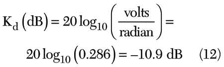
Calibration is relatively simple. The value of Kd is determined by the phase shifting one path by a known amount and measuring the corresponding voltage change at the mixer. This is done at DC and assumed to be valid at the carrier offset. Most mixers are flat to within a tenth or two of a dB in the DC to 1 MHz range. For example, if a 2° phase shift is introduced, or 0.035 radians, and a DC voltage change of 10 mV is measured, then the corresponding phase detector constant of 0.286 is calculated by dividing the volts by the radians. In terms of voltage, it can be converted into dB as
The voltage noise is usually specified in terms of dB and the phase noise relation to the measured voltage noise can be rewritten as

If Sv is measured to be –165 dBV, using a phase detector constant (Kd) of –10.9 dB, then the resulting single sideband phase noise is –157.1 dB.
The Effects of Compression on the Large-signal Noise Figure

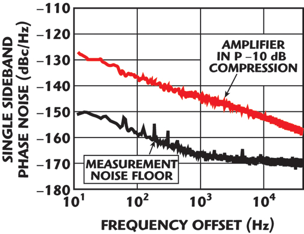
How a small-signal noise figure can be related to the additive phase noise when an amplifier is driven in a very linear region has been shown. What happens when an amplifier is driven into compression? Figure 4 shows the same sample amplifier measured previously, but driven into 1 dB compression with an output of 19 dBm. The flicker corner has increased and the noise at offsets of less than 10 kHz has increased by approximately 10 dB. Figure 5 shows the amplifier in deep compression and fully saturated at 20 dBm output. The flicker corner is beyond the audio card measurement bandwidth and the noise has been degraded by an additional 10 dB. This amplifier was powered by a battery pack and well bypassed, so that the measurement result is due strictly to the self noise of the amplifier. These figures show how the measurement of additive phase noise provides more effective information than using the small-signal noise figure.
Industry trends have been to improve amplifier efficiency, especially in high power amplifiers, which generally means operating in deep saturation. From these measurements, it can be concluded that the additive noise may be significant to the overall system performance. What has not been demonstrated are the effects of bias voltage noise on the overall phase noise when operating in deep compression. In deep compression, amplifiers go through a dramatic phase change as the drain voltage varies. This causes a large AM-PM conversion and any noise on the bias line will be heavily up-converted to the carrier frequency and measured as phase noise.3
Additive Noise or Noise Figure of Frequency Translation Devices
Now consider an additive phase noise measurement for a frequency multiplier or a frequency divider. The only way to calculate the noise added by those devices is through an additive phase noise measurement. Virtually all frequency multipliers and dividers are driven in large signal for correct operation and the noise figure has absolutely no meaning in the traditional sense. These devices are used along the signal path and can degrade the overall signal-to-noise ratio of the system and it is important to know by exactly how much. This is especially true for active frequency multipliers or dividers, which tend to be much noisier than their passive counterparts. Figure 6 shows the measurement set-up used to measure the additive phase noise in frequency translating devices. The phase detector only works at a given frequency for both paths. Therefore, changes must be made identically to both paths in the measurement set-up, so that the phase detection frequency is identical for both the RF and LO ports. In this regard, frequency translation devices are always measured as a pair. The overall noise power measured is twice that of an individual device, assuming they exhibit identical noise amplitude and the noise is uncorrelated. If multiple devices are measured, then the individual contribution of any one device can be found.

When measuring a single pair of devices, there are two unknowns (the phase noise of each device) and one known (the phase noise for the pair). Inherently, there is a 3 dB uncertainty in the measurement of two devices. The noise may be equal between both DUTs or entirely due to one.
The phase shift for calibration is determined for the phase comparison frequency and the input frequency is irrelevant. To that extent, the frequency multiplication or division may be of any ratio, provided both paths are identical. A notable complication with additive phase noise measurements of frequency translation devices is related to the drive power of the mixer or phase detector. A frequency doubler may output less than 0 dBm, not enough to drive the LO of the mixer, so an amplifier is required to provide gain to the signal prior of the mixer, which may add phase noise to the overall measurement. Careful selection of a proper amplifier and good characterization can reduce this effect to an extremely low level.
Baseband Analysis and Phase Detectors
Voltage noise measured at the IF port of the mixer is very close to the thermal noise floor of the load impedance presented to the mixer. A 50 Ω resistor exhibits a noise of less than 1 nV/Hz. To that extent, an analog to digital converter (ADC) cannot measure down to the appropriate level and the signal must be amplified into the range of the ADC. The requited gain can vary from 20 to 60 dB or, in terms of voltage, 10x to 1000x, depending on the noise level to be amplified and the dynamic range of the ADC. Even the best FFT analyzers cannot measure down to this level without some external amplification. Most engineers seek data from 10 Hz to approximately 1 MHz, although 100 Hz to 100 kHz is often sufficient.
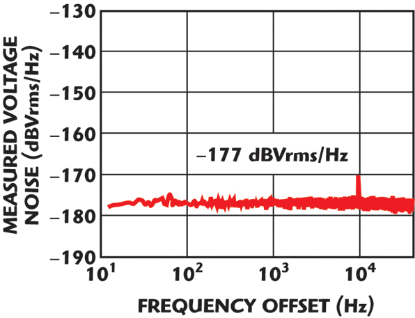
A good low noise amplifier exhibits a self noise near 1 nV/Hz, which is enough to degrade the noise due to even a 50 Ω resistor only marginally. Furthermore, it has a bandwidth that will extend to at least the highest desired measurement. A low cost way to do phase noise measurements to 40 kHz is to use a good LNA in conjunction with a high performance audio card as an FFT analyzer. Most high-end audio cards sample at up to 96 ksps with a bandwidth that extends from 20 Hz to 40 kHz and very often extend down to 10 Hz with only 1 to 2 dB of attenuation. All the measurements for this article were made using the LNA plus audio card method. A copy of the Matlab™ script used to perform these measurements can be made available upon request to the authors (support@holzworth.com). Figure 7 shows the voltage noise floor of an audio card using a low noise amplifier that exhibits a 1 nV/Hz.
A note on frequency translation devices: typically, these devices contain high levels of harmonics, both sub harmonics and higher harmonics. Digital frequency dividers have a square wave output, causing very high third, fifth and higher harmonics. Analog frequency dividers may have strong sub harmonics and associated harmonics. If these harmonics are within 20 dB of the desired signal to be measured, it can affect the accuracy of the measurement. Under this scenario, it is advised that the desired frequency be filtered out so as to not adversely affect the measurement.
Mixers as Phase Detectors
Not all mixers are created equal (as phase detectors), not even double balanced mixers. LO-RF and LO-IF isolation, conversion efficiency, IF bandwidth and IF circuitry, and even the type of diode used affect how a mixer operates as a phase detector. There are many variables and whenever a new mixer is selected as a phase detector, a series of measurements should be completed to determine noise floor, compression levels and a range of calibration constants. Having a well characterized mixer can give an early indication of a bad calibration or a poor test set-up, if the calibration constant is significantly different from the expected value.
A good phase detector will exhibit a noise floor of –170 dBc/Hz, even if driven by a nearly perfect synthesizer and will always exhibit some flicker noise. A final note that phase detectors demonstrate a limited signal-to-noise ratio when acting as phase detectors: first, the LO drive level must be sufficient to turn the diodes on. The RF signal is then multiplied by the LO and passed onto the IF port with some conversion efficiency. Assuming that the output voltage at the IF is approximately 424 mVrms when sweeping the phase 360° (600 mV peak voltage), the LNA has a self noise of approximately 1 nV/Hz. If a 50 ω resistor is used to terminate the mixer, then the overall noise will be approximately 1.4 nV/Hz at the LNA. Taking the ratio of 1.4 nV/424 mV results in a –169.6 dBc/Hz noise floor. To improve the SNR of the measurement, a larger RF drive must be used, but at some point the mixer compresses and will no longer improve the SNR, actually hindering it by adding shot noise from the mixer and degrading the flicker noise corner.
Many manufacturer application notes indicate that using a high impedance to terminate the mixer (anywhere from 1 to 5 kω) instead of a standard 50 ω will improve the sensitivity, but the phase detector constant will at most double. The mixer diodes exhibit a self noise of a few hundred ohms to 1 kω and the increase in voltage noise of the equivalent resistance at the IF port increases the noise floor. This will cancel any increase in the phase detector constant, which results in approximately the same SNR. Finally, when terminating a mixer with something other than 50 ω, the isolation of the mixer may be degraded and the overall phase noise performance reduced.
Conclusion
This article has presented additive phase noise as an element inherent in all two-port devices. Simple and economical means to measure additive phase noise in amplifiers, multipliers and dividers have been shown. Once the effort has been made to apply the equations presented, the additive phase noise measurement can become an integral part of every R&D and manufacturing test line.
References
1. A. Hati, D.A. Howe, F.L. Walls and D. Walker, “Noise Figure vs. PM Noise Measurements: A Study at Microwave Frequencies,” 2003 IEEE International Frequency Control Symposium Proceedings.
2. F.L. Walls, “Correlation between Upper and Lower Sidebands,” IEEE Transactions on Ultrasonics, Ferroelectrics and Frequency Control, Vol. 47. No. 2, March 2000, pp. 407–410.
3. J. Breitbarth, S. Pajic, N. Wang and Z Popovi, “Additive Phase Noise in Linear and High-efficiency X-band Power Amplifiers,” 2006 IEEE MTT-S International Microwave Symposium Digest, pp. 1871–1874.
4.M.M. Driscoll and T.D. Merrell, “Spectral Performance of Frequency Multipliers and Dividers,” 1992 IEEE Frequency Control Symposium, pp. 193–199.
5.G.K. Montress, T.E. Parker and M.J. Loboda, “Residual Phase Noise Measurements of VHF, UHF and Microwave Components,” IEEE Transactions on Ultrasonics, Ferroelectrics and Frequency Control, Vol. 41, No. 5, September 1994, pp. 664–679.
Jason Breitbarthreceived his BSEE degree from Oregon State University in 1997, and his MS and PhD degrees in electrical engineering from the University of Colorado in 2001 and 2006, respectively. Past professional experience includes working for Agilent Technologies and Picosecond Pulse Labs. He is the founder of Holzworth Instrumentation. His current efforts include architecting extremely small, ultra-low phase noise synthesizers and phase noise test equipment.
Joe Koebel received his BSEE from Michigan Technological University in 1994 with an emphasis on electromagnetics and communications theory. Past professional experience includes working for Hughes Space & Communications (now Boeing Satellite Systems) and Picosecond Pulse Labs. He is currently a cofounder and VP of sales & marketing for Holzworth Instrumentation.