Personal wireless communications have recently gained wide popularity. Presently, the trend is to provide a wireless link to every kind of electronic device. In particular, there is a specific need for greater capacities and transmission speeds, which, together with a growing demand from users for more complicated services, require the design of higher performance systems.
In this context, multi- and wideband antennas are required. Many researchers have investigated the design of multi-band antennas to cover different frequency ranges.1–5 Other researchers investigated techniques to improve the antenna bandwidth.6–11
On the other hand, a small antenna size is required to meet the miniaturization requirements of the mobile communication system. Several methods have been used to miniaturize microstrip antennas such as loading the microstrip patch with a high dielectric substrate, short circuiting the microstrip patch to the ground plane, modifying the basic microstrip patch structure, or using a meander line.12-14
In this article, a compact antenna is presented, which operates in several frequency bands in the range between 0.5 and 3 GHz including GSM 900, GSM 1800, GSM 1900, UMTS-2110, and the industrial, scientific and medical (ISM) band around 2.4 GHz, as well as WLAN and Bluetooth applications operating at 2.4 GHz. The proposed antenna consists of a microstrip feedline, a two-step power coupler, a rectangular loop and a meander line, which is connected to the loop at certain positions.
The meander line is used to decrease the antenna size, and all these components together provide multi-paths for the current, resulting in multiple resonances. The proposed antenna belongs to a category similar to the one described by Thakur, et al.14 However, the antenna here has only one port, and provides more operating frequencies.
The simulation and analysis for the present antennas were performed using the commercial computer software package, Ansoft HFSS, which is based on the finite element method. A prototype was manufactured and measured and a good comparison between measurements and simulations is obtained.

Antenna Geometry and Analysis
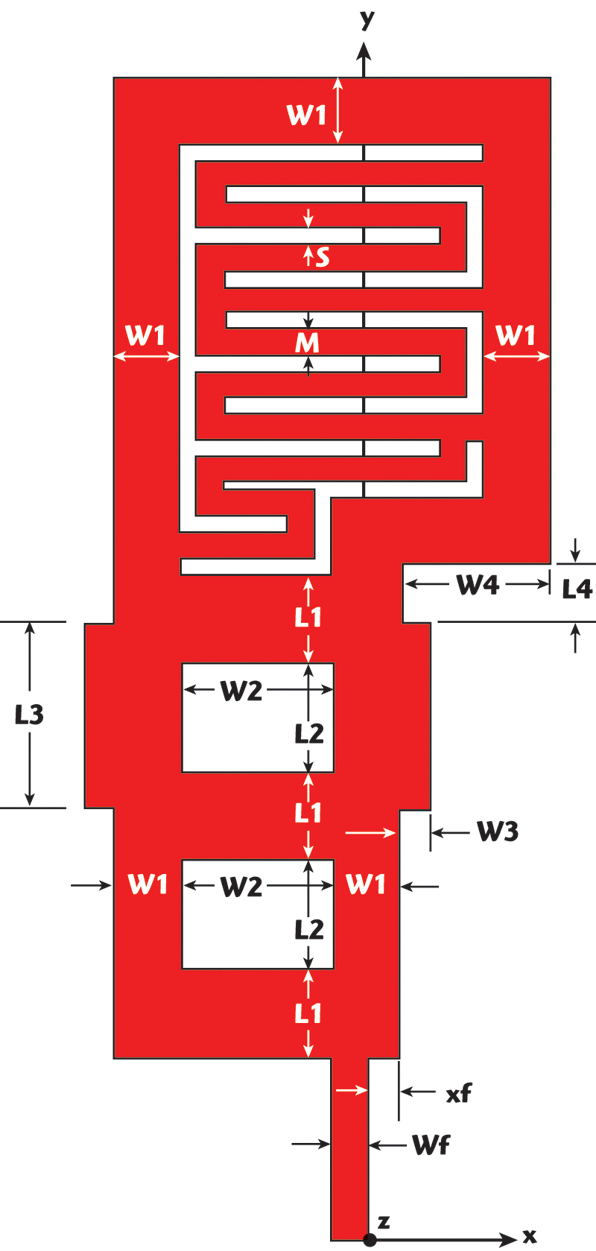
The geometry of the proposed antenna is shown in Figure 1. The antenna is built on an FR4 epoxy substrate of height h = 1.6 mm and dielectric constant ε = 4.4. The right, left and top edges of the substrate are 3 mm away from the edges of the antenna.
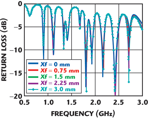
The antenna is fed by a 50 Ω microstrip line of width Wf and is placed at distance xf from the lower right corner of the antenna. The length of the microstrip line is 16 mm.
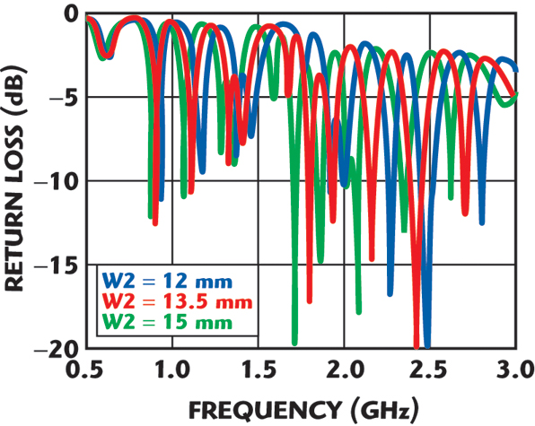
The antenna consists of two consecutive power couplers to excite different modes and provide different current paths. They are defined by the parameters W1 and W2 in the x-direction, and L1 and L2 in the y-direction. A stub is added to the second coupler for matching, and is defined by the parameters W3 and L3.
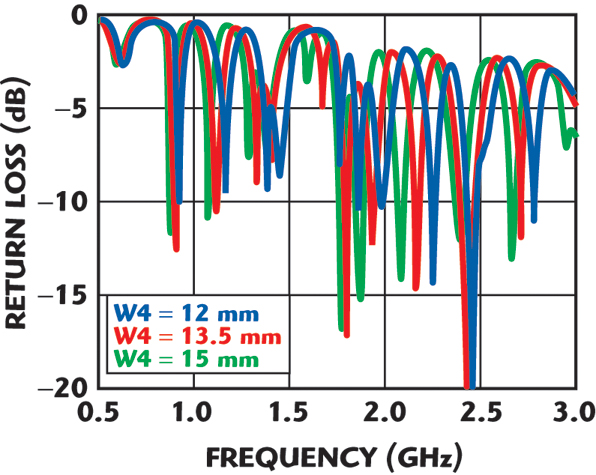
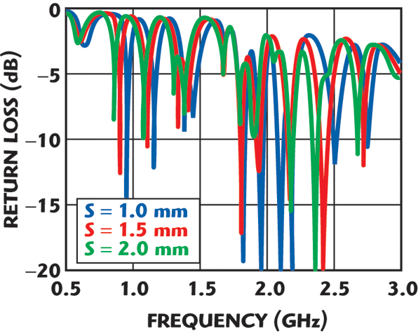
The power couplers are then connected to a microstrip loop of width W1. The right lower corner of the loop is defined by the parameters W4 and L4. A meander line is placed within the loop to efficiently fill the entire space. The meander line width is M and the distance between the lines is S. Short circuits between the loop and the meander line are added to provide extra current paths.
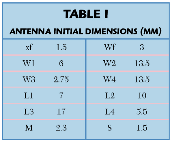
Based on an extensive preliminary study of this antenna, the initial design is chosen to have the dimensions shown in Table 1.
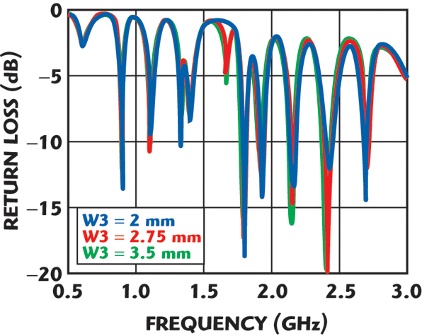
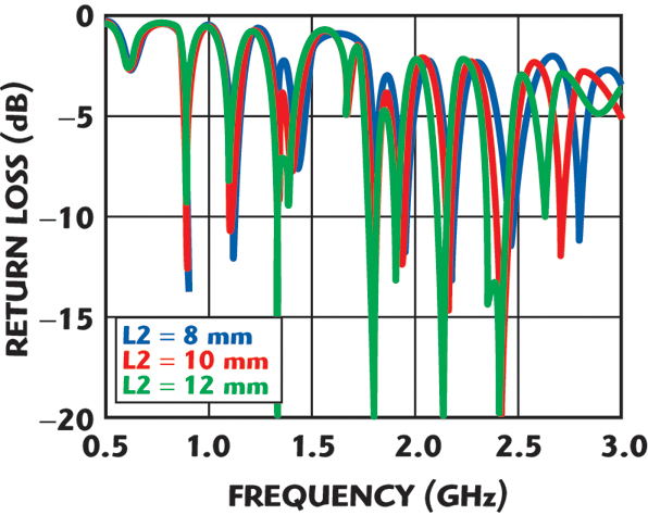
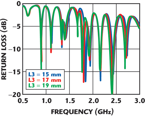
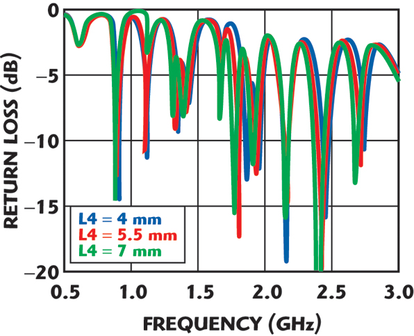
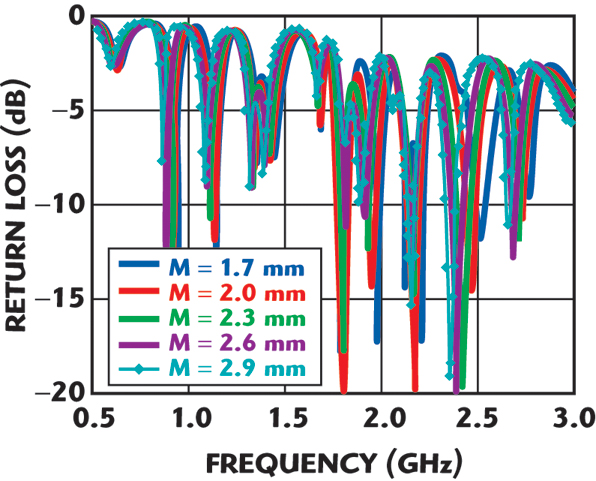
The parameters of the antenna are studied by changing one parameter at a time, while keeping the other parameters constant. The results are shown in Figures 2 to 12 for the W, L, M, S and xf parameters, respectively. Generally, increasing all parameters decreases all the resonance frequencies of the antenna because this increases the antenna size.
The parameter W3 controls the level of the return loss because it affects the S-parameters of the second coupler, which lies between the loop and the meander in one side, and the feedline and the first coupler in the other side, and consequently affects the matching between them.
Final Antenna Results
The final design of this antenna has L1 = 8 mm and xf = 0; the other parameters are the same as in Table 1. This antenna was manufactured using a milling machine and measured using an Agilent E5071B network analyzer (ENA series) in the Oak Ridge National Laboratory. A prototype of the antenna is shown in Figure 13.
The measured and computed return loss of this antenna are shown in Figure 14 from 0.5 to 3 GHz. A good agreement is obtained between measurements and simulations which verify the results obtained by HFSS for the proposed antenna design, and shows the low sensitivity to the manufacturing tolerances.

In simulation, the antenna has nulls at 0.9, 1.11, 1.34, 1.39, 1.67, 1.82, 1.92, 2.14, 2.43 and 2.65 GHz, while the measurements show that the antenna operates at 0.89, 1.09, 1.32, 1.38, 1.66, 1.8, 1.91, 2.15, 2.4 and 2.61 GHz. The small differences between the two results are caused by the SMA connector, the inaccuracy of the milling machine and the uneven substrate surface which results from peeling off the copper.
The antenna size (47.75 mm) compared to the wavelength at the lowest operating frequency is only 0.14λ0. These results prove that this antenna is a good candidate for many wireless applications such as GSM 900, GSM 1800, GSM 1900, UMTS-2110, and the industrial, scientific and medical (ISM) band around 2.4 GHz, as well as WLAN and Bluetooth applications operating at 2.4 GHz.
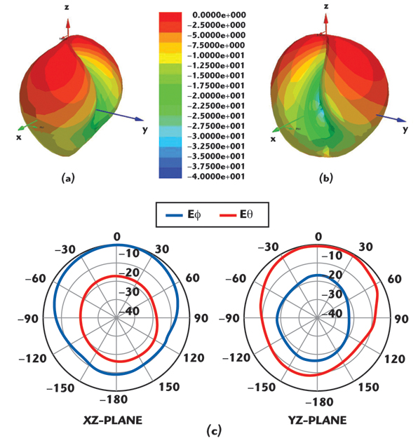
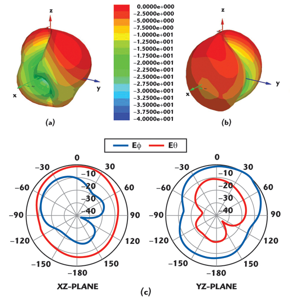
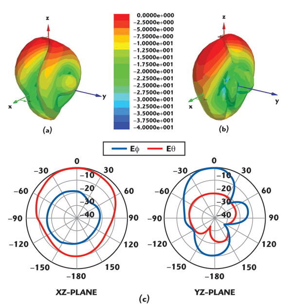
The computed magnitude and vector surface current distributions at 0.9, 1.9 and 2.4 GHz are shown in Figure 15. A combination of two or more elements of the antenna provides each of these three resonances. The 2D and 3D radiation patterns are calculated using Ansoft HFSS at 0.9, 1.9 and 2.4 GHz and are presented in Figures 16 to 18.
The radiation patterns at the three frequencies are almost similar to each other. The only clear difference is in the polarization, where the antenna is quasi y-polarized at 0.9 GHz, and quasi x-polarized at 1.9 and 2.4 GHz, which is due to the difference in the excited mode.
Conclusion
A compact microstrip antenna fed by a single microstrip line has been proposed and analyzed for multi-band wireless communications applications. The prototype of the antenna has been designed using Ansoft HFSS and realized through measurements.
The presented antenna has a compact size of 0.14λ0 at 0.9 GHz. Similar radiation patterns are obtained at 0.9, 1.9 and 2.4 GHz. This antenna can be easily integrated into and accomplish the requirements of modern mobile communication systems.
Acknowledgment
The author would like to thank the RF and microwave group of the Oak Ridge National Laboratory, Oak Ridge, TN, for its great support and help in building and measuring the proposed antenna in this article.
References
1. R.L. Li, G. Dejean, M.M. Tendtzeris and J. Laskar, “Novel Multi-band Broadband Planar Wire Antenna for Wireless Communication Handheld Terminals,” 2003 IEEE Antennas and Propagation Society International Symposium Digest, Vol. 3, pp. 44–47.
2. P. Nepa, A.A. Serra, S. Marsico and G. Manara, “A Dual-band Antenna for Wireless Communication Terminals,” 2004 IEEE Antennas and Propagation Society International Symposium Digest, Vol. 4, pp. 4284–4287.
3. E.S. Angelopoulos, A.I. Kostaridis and D.I. Kaklamani, “A Novel Dual-band D-inverted Antenna Printed on a PCMCIA Card,” Microwave Optical Technology Letters, Vol. 42, No. 2, July 2004, pp. 153–156.
4. C.M. Allen, A.A. Eldek, A.Z. Elsherbeni, C.E. Smith, C.W. Huang and K.F. Lee, “Dual-tapered Meander Slot Antenna for Radar Applications,” IEEE Transactions on Antennas and Propagation, Vol. 53, No. 7, July 2005, pp. 2324–2328.
5. A.A. Eldek, A.Z. Elsherbeni and C.E. Smith, “Dual-wideband Square Slot Antenna with a U-shaped Printed Tuning Stub for Wireless Communication Systems,” Progress in Electromagnetics Research, PIER 53, 2005, pp. 319–333.
6. A.A. Eldek, A.Z. Elsherbeni, C.E. Smith and K.F. Lee, “Wideband Rectangular Slot Antenna for Personal Wireless Communication Systems,” IEEE Antennas and Propagation Magazine, Vol. 44, No. 5, October 2002, pp. 146–155.
7. X.C. Lin and L.T. Wang, “A Broadband CPW-fed Loop Slot Antenna with Harmonic Control,” IEEE Transactions on Antennas and Wireless Propagation Letters, Vol. 2, 2003, pp. 323–325.
8. J.Y. Chiou, J.Y. Sze and K.L. Wong, “A Broadband CPW-fed Strip-loaded Square Slot Antenna,” IEEE Transactions on Antennas and Propagation, Vol. 51, No. 4, April 2003, pp. 719–721.
9. H.D. Chen, “Broadband CPW-fed Square Slot Antennas with a Widened Tuning Stub,” IEEE Transactions on Antennas and Propagation, Vol. 51, No. 8, August 2003, pp. 1982–1986.
10. N. Behdad and K. Sarabandi, “A Multi-resonant Single-element Wideband Slot Antenna,” IEEE Transactions on Antennas and Wireless Propagation Letters, Vol. 3, 2004, pp. 5–8.

11. J.Y. Sze and K.L. Wong, “Bandwidth Enhancement of a Microstrip-line-fed Printed Wide-slot Antenna,” IEEE Transactions on Antennas and Propagation, Vol. 49, No. 7, July 2001, pp. 1020–1024.
12. K.L. Wong, Compact and Broadband Microstrip Antennas, John Wiley & Sons Inc., New York, NY, 2002.
13. K. Fujimoto and J.R. James, Mobile Antenna Systems Handbook, Second Edition, Artech House Inc., Norwood, MA, 2000.

14. J.P. Thakur, J.S. Park, B.J. Jang and H.G. Cho, “Small Size Quad-band Microstrip Antenna,” Microwave Optical Technology Letters, Vol. 49, No. 5, May 2007, pp. 997–1001.

Abdelnasser A. Eldek received his BSc degree in electronics and communications engineering from Zagazig University, Egypt, in 1993, his MS degree in electrical engineering from the Eindhoven University of Technology, Eindhoven, The Netherlands, in 1999, and his PhD degree in electrical engineering from the University of Mississippi in 2004. He was a research assistant in the department of microwaves, Electronic Research Institute, Cairo, Egypt, from 1995 to 1996. From January 2001 to December 2004, he was a research and teaching assistant in the department of electrical engineering at the University of Mississippi.

He is currently an assistant professor in the department of computer engineering, Jackson State University, Jackson, MS. His main research areas include electromagnetics, antennas, phased arrays, RF/microwave circuits and numerical methods.