
In order to improve the simulation accuracy of microwave circuit designs, an accurate active device model plays an important role for circuit simulations. According to previous studies, the BSIM models can precisely predict the characteristics of deep sub-micron MOSFETs at operation frequencies below 1 GHz for digital and analog circuit designs.1 However, it cannot completely describe device behaviors at operation frequencies above several gigahertz, particularly the nonlinear behaviors and parasitic effects.2 To develop a complete MOSFET RF large-signal model, an extended RLC network representing the parasitic effects of layout and the lossy substrate must be added into the standard BSIM model for obtaining more accurate modeled results.3–5 In case these parasitic effects are not taken into account in a RF model, the fitting results will be only limited to several gigahertz, especially on S-parameters and power characteristics.
As to the extraction for parasitic resistances/inductances at each terminal, these parameters can be directly extracted by the proposed method.6 According to previous studies,7,8 it shows a reliable demonstration in their experimental results. In addition to the extrinsic parasitic resistances/inductances, the lossy substrate becomes more significant due to the power loss from thinner bulk material in deep sub-micron CMOS technologies. Thus, a new equivalent-circuit for lossy substrates has been proposed8 to simulate the lossy parasitic effects through gate/drain terminals, which can accurately capture the unique frequency response associated with the lossy substrate. Although a good agreement has been realized between measured and modeled results in terms of S-parameters and NFmin,8 the proposed extraction procedure is very difficult and inconvenient because it requires a complicated curve-fitting approach and the accuracy depends on the fitted range of data. Besides, only S-parameter fitting results were shown and nonlinearity prediction was not included. In order to eliminate the curve-fitting process, a simple extraction method for the lossy substrate has been reported in this article. This new extraction method does not need the complex calculations and curve-fitting processes that can extract the parameters for lossy substrate networks. In this work, an improved BSIM4 large-signal model for a 0.13 μm CMOS device is presented by using a new extraction method, and verified by S-parameters for operation frequencies up to 40 GHz plus the DC I-V, low-frequency noise and power characteristics.
Extraction Method
A 0.13 μm NMOS transistor with a total gate-width of 200 μm was measured and extracted in this article. The device layout is employed by a multi-finger structure with a finger width of 5 μm and a finger number of 40. Microwave S-parameters were measured on-wafer using a E8364A network analyzer from 0.1 to 40.1 GHz, and the de-embedding “open” pad was used to remove the pad parasitic effects. In order to improve the RF large-signal model, the parasitic effects of layout and lossy substrate must be taken into account for accurate S-parameter prediction. Figure 1 shows a simple small-signal equivalent-circuit model for a MOSFET. This equivalent-circuit mainly consists of two parts, intrinsic and extrinsic. The intrinsic part represents the characteristics for the transistor core, which can be well predicted by the BSIM model. The extrinsic part, representing the parasitic resistance/inductance from physical layout, plays an important role for fitting S-parameters at high frequencies. However, the gate resistance Rg represents the distributed gate resistance, and Rd and Rs represent the contact and sheet resistances for drain and source terminals that is related to the diffusion area. Three parameters of Lg, Ld and Ls are the series parasitic inductances in each terminal from metal connections. In this study, a proposed extraction method was used for obtaining these extrinsic parameters.6 The above equivalent-circuit shown in the figure can be expressed by the following Z-parameters:


where

is the calculated Y-parameter results of the intrinsic part. In the case where the real and imaginary parts in Equations 1 to 4 are considered individually, the extrinsic resistances and inductances can be derived by the following equations:

where B, Ag, Ad, As, Eg, Ed, Es and Fg are expressed as functions of intrinsic parameters and constant values under a fixed bias condition.
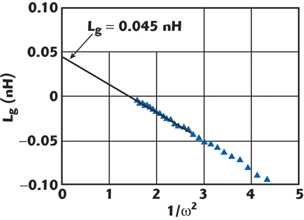
At much higher frequencies, ω2 is much greater than B in Equations 5 to 10. B can be significantly reduced by minimizing gm and gds at the zero Vgs bias condition, so the frequency dependent terms related to the intrinsic part are much smaller than the extrinsic terms in previous equations. Thus, the extrinsic resistances and inductances can be extracted as ultimate values at an infinite frequency. Figure 2 plots the measured data of Re(Z22–Z12) against 1/ω2, which means the gate resistance Rg can be obtained with a value of 3.5 Ω by using a linear regression method to find the y-intercept of Re(Z22–Z12) against 1/ω2 at an infinite frequency. Figure 3 also demonstrates the extracted gate inductance Lg of 0.045 nH from the y-intercept of (1/ω)Im(Z11–Z12) against 1/ω2. As for the other parameters, the same extraction method was used where the extracted Ld = 0.04 nH, Rd of 2 Ω, Ls = 0.02 nH and Rs = 1.5 Ω.
With regard to the substrate network, the standard BSIM4 model offers a built-in substrate network. However, this substrate network does not have the ability to describe the nonlinear frequency dependent characteristics due to its construction by resistance only,1 so that the published paper8 proposed a series RLC in parallel with a capacitance to accurately predict the behavior of the silicon lossy substrate. Therefore, to obtain the parameters of this network, an “open” pad is used for extraction of these values in this article.

The proposed equivalent-circuit model for an “open” pad is shown in Figure 4. It consists of a RLC network incorporating the pad capacitance Cpad and substrate parameters Rsi, Csi, Lsi and Cp. The pad capacitance Cpad is used to model the dielectric capacitance under the signal pad, which is mainly dominated by the pad size and thickness between the metal and the substrate layer. The main substrate parameters Rsi, Csi, Lsi and Cp connected from gate/drain to ground are used to simulate the silicon lossy substrate. Capacitances Cp and Csi account for the capacitive coupling while substrate resistance Rsi and Lsi were proposed to model the semi-conducting nature of the silicon substrate at high frequency operation. The parameters of Csi, Rsi and Lsi are three key parameters to capture the lossy substrate feature up to 40 GHz. The Csi is the primary component for the phase deviation and nonlinear response in lower frequencies, and Lsi reveals increasing these effects at higher frequencies.
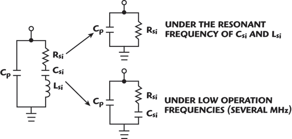
In the work, the Cpad value of 160 fF is a calculated parameter by physical process and layout rather than from extraction. After de-embedding the pad capacitance Cpad, the measured Z-parameters of the lossy substrate can be obtained from the S-parameter transformation. The first step of the proposed extraction method is to assume the series Csi and Lsi can be considered as a short circuit at their resonant frequency, and the effect of this series LC can be removed from this network. As shown in Figure 5, the RLC substrate network is simplified to one capacitance Cp in parallel with Rsi. Therefore, both parameters Cp and Rsi can be directly extracted from the substrate network. Figure 6 plots the measured Z-parameters for an open pad after de-embedding the pad capacitance. In this figure, a minimum value found at 27.1 GHz, which was representing the Rsi value of 237.5 Ω, since the series Csi and Lsi were eliminated at their resonant frequency. The Cp value of 18.59 fF was extracted from the Im(Z11) at the same resonant frequency of 27.1 GHz. This information can also be obtained in Figure 6.

After extracting the Cp and Rsi, two unknown parameters Csi and Lsi still exist. Therefore, the second step of our extraction method is to assume the Lsi can be omitted at very low frequencies such as several megahertz. The equivalent-circuit for the lossy substrate can be simplified to Figure 5, and the Csi at such low frequencies can be expressed by

According to Equation 11, Csi can be determined by the extracted Cp, Rsi and measured Z-parameters at 10 MHz, which was determined to be 216 fF. Finally, the last unknown parameter Lsi can easily be calculated from the resonant frequency f0 = 1/2π√LsiCsi, and the Lsi value is 0.16 nH.

Improved BSIM4 Model
The BSIM model is a standard model widely used in sub-micron MOSFETs for general circuit designs below 1 GHz. Recent works have demonstrated that it is capable up to several gigahertz by adding RLC networks to represent the parasitic effects at higher frequencies.3-5 Providing the device channel length is scaled down to deep sub-micron technologies, the combined effects of ever-shortened channel devices and millimeter-wave operation frequencies become a major challenge for device modeling. However, the BSIM4 model provides good predictions for short-channel effects under high supply voltages which are related to the output power at microwave frequencies and have better descriptions for some RF behaviors by high-frequency correlation parameters.1 In response to this situation, it is proposed to adopt the BSIM4 model as the intrinsic core for DC I-V characteristics prediction and add RLC networks incorporating the parasitic effects of layout and lossy substrate to accurately accomplish a large-signal RF CMOS model.
The proposed equivalent-circuit model of a 0.13 μm NMOS transistor is shown in Figure 7. The fully equivalent-circuit contains an intrinsic core M1 as represented in the original BSIM4 model. The BSIM4 model was transferred and modified through the BSIM3 model provided by the foundry. The RLC networks at each terminal are the extrinsic resistances/inductances and lossy substrate, which represent the high-frequency parasitic effects associated with practical layout and process. All parameters were extracted by the extraction methods discussed in this article. The optimization was done by using the Agilent ADS simulator to achieve the best fitting results on S- and Y-parameters.
Results and Discussion
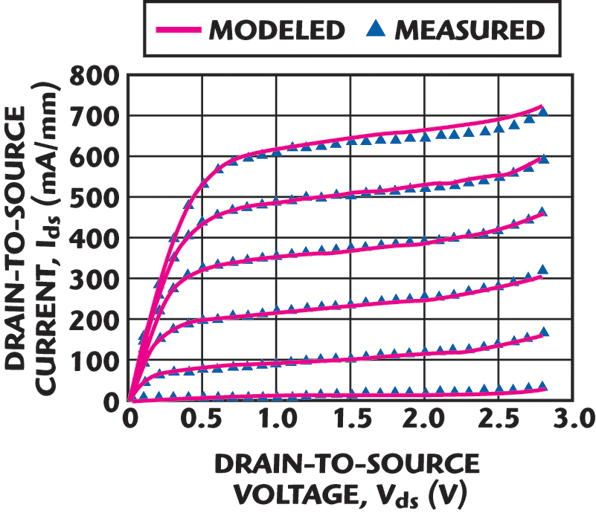
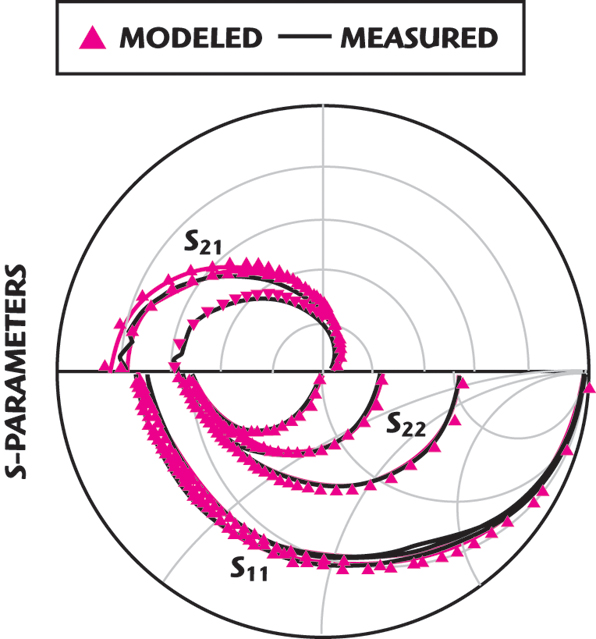
The 0.13 μm NMOS transistor with 200 μm gate-width fabricated by Taiwan Semiconductor Manufacturing Co. (TSMC) CMOS 1P8M standard process was measured and modeled for DC I-V, S-parameters, low-frequency noise and load-pull power characteristics. Figure 8 shows the measured and modeled DC I-V characteristics, while Vgs was 0.4 to 1.4 V with steps of 0.2 V, and Vds was 0 to 2.8 V. The predicted DC I-V characteristics were done by the BSIM4 model and matched well to the experimental data. This result is very important for mixer and power amplifier designs due to the nonlinearly knee-voltage and breakdown-voltage regions that are the key factors to the nonlinear circuits. Figure 9 plots the transconductance (gm) of this device; a normalized peak gm of 650 mS/mm was obtained under a Vgs of 0.8 V. The extracted fT and fMAX under peak gm condition are 96 and 55 GHz, respectively. Figure 10 shows the measured and modeled results of S-parameters up to 40 GHz under biased voltages Vds of 1 V, and Vgs 0.6 to 1.4 V with steps of 0.4 V. This figure indicates that the S-parameters with bias-dependent conditions can be predicted well by the proposed model. In case the lossy substrate networks are not included in this model, the accuracy of the S-parameter is limited to only several gigahertz. Figure 11 shows the low-frequency noise characteristics at Vds of 1 V with a biased current of 10 mA. This result is extracted by the SPICE-Flicker equation,9 that is given by


where KF is flicker noise coefficient, and AF and EF are flicker noise exponent and frequency exponent. This 1/f noise expression in BSIM4 is identical with that in BSIM3, except for the definition of oxide thickness. The BSIM4 adopts the electrical oxide thickness for the most of its capacitance calculations (Cox,e). In addition to the device’s DC I-V, S-parameters and low-frequency noise verification, the evaluation of large-signal performance at 5.8 GHz at Vds of 1 V with a biased current of 50 mA was also conducted. Figure 12 plots power gain (Gp) and output power (Pout) as a function of input power (Pin) for measured and modeled results. In this figure, the model with the lossy substrate shows a well matched trend with the measured data, with a linear power gain of 12.4 dB and a 1 dB compression point of 0 dBm. The traditional model without the lossy substrate achieves higher Gp and Pout compared to the measured results, due to the model that cannot precisely simulate the power loss without substrate leakage current and parasitic effects considerations. Furthermore, the two-tone test was performed at frequencies of 5.800 and 5.801 GHz, as shown in Figure 13, that plots the verification results of third-order inter-modulation (IM3) and output power versus Pin. This figure demonstrates not only that the fundamental output power can be well predicted, but also the IM3 output power, which is helpful for harmonic predictions in large-signal circuits. These results demonstrate good agreement between the predictions of the improved BSIM4 model and the measurement of the experimental characterization.
Conclusion
According to the obvious short-channel effects in advanced CMOS technology, the BSIM4 model achieves better predictions compared to the BSIM3. The additional RLC networks representing the extrinsic resistances/inductances and lossy substrate must be taken into account for employing the deep sub-micron CMOS devices into microwave circuit designs. To accurately obtain the lossy substrate parameters, a simple extraction method without any complicated calculations and curve-fitting processes is proposed in this article. A 0.13 μm NMOS transistor was measured and extracted in terms not only for S-parameters, but also DC I-V, low-frequency noise and power characteristics. Excellent agreement has been obtained between measured and modeled results. This accurate model is useful for operation frequencies up to 40 GHz to improve the simulation accuracy in microwave applications.

Acknowledgment
The authors would like to thank the Taiwan Semiconductor Manufacturing Co. (TSMC) for providing the foundry service through the National Chip Implementation Center (CIC), and Nano Device Labs (NDL) for power and noise measurements. This work was supported in part by the National Science Council, ROC, under Contract No. NSC95-2221-E-182-071.
References
1. W. Liu, MOSFET Models for SPICE Simulation Including BSIM3v3 and BSIM4, Wiley, 2001.
2. Y.H. Cheng, M.J. Deen and C.H. Chen, “MOSFET Modeling for RF IC Design,” IEEE Transactions on Electron Devices, 2005, pp. 1286–1303.
3. C. Enz, “An MOS Transistor Model for RF IC Design Valid in All Regions of Operation,” IEEE Transactions on Microwave Theory and Techniques, 2002, pp. 342-359.
4. C.W. Kuo, C.C. Hsiao, C.C. Ho and Y.J. Chan, “Scaleable Large-signal Model of 0.18 CMOS Process for RF Power Predictions,” Solid-State Electronics, 2003, pp. 77–81.

5. H.H. Lai, C.C. Hsiao, C.W. Kuo, Y.J. Chan and T. Sato, “Improved CMOS Microwave Linearity Based on the Modified Large-signal BSIM Model,” IEICE Transactions Electron, 2004, 87-C, pp. 76–80.
6. S. Lee S, H.K. Yu, C.S. Kim, J.G. Koo and K.S. Nam, “A Novel Approach to Extracting Small-signal Model Parameters of Silicon MOSFETs,” IEEE Microwave and Guided Wave Letters, 1997, pp. 75–77.
7. S. Lee, C.S. Kim and H.K. Yu, “A Small-signal RF Model and its Parameter Extraction for Substrate Effects in RF MOSFETs,” IEEE Transactions on Electron Devices, 2001, pp. 1374–1379.
8. J.C. Guo and Y.M. Lin, “A New Lossy Substrate De-embedding Method for Sub-100 nm RF CMOS Noise Extraction and Modeling,” IEEE Transactions on Electron Devices, 2006, pp. 339–347.
9. J.L. Zhou, M. Cheng and L. Forbes, “SPICE Models for Flicker Noise in N-MOSFETs from Subthreshold to Strong Inversion,” IEEE Transactions on Computer-aided Design of Integrated Circuits and Systems, 2001, pp. 763–767.


Chien-Cheng Wei received his BS degree in electrical engineering from Chinese Culture University, Taipei, Taiwan, ROC, in 2002, and his MS degree in electronic engineering from Chang Gung University, Tao-Yuan, Taiwan, ROC, in 2004. He is currently pursuing his PhD degree in electronic engineering at Chang Gung University. His interests include RF CMOS large-signal device modeling, RF measurement, ultra-wideband integrated circuits and millimeter-wave integrated circuits.

Hsien-Chin Chiu received his BS and PhD degrees in electrical engineering from National Central University, Chungli, Taiwan, ROC, in 1998 and 2003, respectively. He then joined WIN Semiconductors Corp., Tao-Yuan, Taiwan, ROC, where he was engaged in the research and development of 6-inch GaAs pHEMTs and related integrated circuits. He joined the faculty of Chang Gung University in 2004.

Wu-Shiung Feng received his BSEE, MSEE and PhD degrees from National Taiwan University, Taipei, Taiwan, ROC, in 1970, 1974 and 1980, respectively. From 1974 to 1979, he was an instructor in the department of electrical engineering at National Taiwan University. From 1980 to 1985, he was an associate professor, as well as a full professor from 1986 to 1998. He is currently chair of the department of electronic engineering and director of the Graduate Institute of Semiconductor Technology, Chang Gung University, Tao-Yuan, Taiwan, ROC.