
The transistor LC oscillator is at the heart of any wireless communications system. Due to their low cost, design simplicity and ease in practical implementation, for example, MOSFET-based oscillators are widely used in modern wireless handset applications. This three-part tutorial highlights the basics of the oscillator circuit design, setting the relationships between the start-up and steady-state operating modes and the device equivalent circuit parameters. The basic DC and RF device operation regions are explained and analyzed in Part I. It is very important for the oscillator noise model to express a clear relationship between the oscillator spectral noise power density and resonant circuit, and active device parameters. Several approaches, including the simple linear Leeson feedback oscillator model, the linear negative resistance oscillator model and the nonlinear Kurokawa model, will be described and analyzed in Part II. A new impulse response model, based on a phase plane approach, which has become very popular recently, will be the subject of Part III.
Operation and Design Principles
In the first part of this tutorial article, the active device regions and modes of DC and RF operations are discussed with emphasis on CMOS devices, resulting in very simple analytical large-signal voltage-current relationships. An analysis of the start-up and steady-state oscillation conditions, based on a matrix technique showing an explicit analytical dependence between the device and feedback parameters, is given for a widely used single-ended oscillator with a parallel resonant circuit based on a simplified device equivalent model. The basic operation principle of a differential cross-coupled tail-biased oscillator is explained in the time domain.
Device Operation Modes
To better understand the oscillator operation and design principles, it is necessary to first start with the basic physics and electrical behavior of the MOS transistor as a main element of the oscillator, whose typical current-voltage (I-V) characteristics are shown in Figure 1. Initially, consider the situation for a fixed gate bias Vgs and an increasing drain-source voltage Vds. As seen for low drain bias voltages Vds, the drain current Id increases almost linearly. This region of the device output DC characteristic is therefore called the linear region. In this case, there is an inversion layer connecting the source and drain, which behaves as an ideal ohmic resistor. Then, at larger drain bias voltages, the dependence of the drain current on the drain bias voltage decreases. Finally, at some voltage, known as the saturation voltage Vsat, the drain current no longer increases with increasing drain-source voltage. This region is called the saturation region, due to the effect of the DC drain current saturation at high drain bias voltages for a certain gate-source bias voltage Vgs. At Vds = Vsat, the channel is pinched off and the inversion layer is no longer affected by the drain voltages. At drain-source voltages below Vsat, the current continues to flow because there is no barrier to transfer carriers traveling down the channel toward the drain. As they arrive at the edge of the pinched-off region, they are pulled across it by the field directed from the drain toward the source. If the drain bias is increased further, any additional voltage is dropped across the depleted, high field region near the drain electrode, and the point at which the channel is entirely depleted moves slightly toward the source.1 Note that at very high gate bias voltages (voltages Vgs(5) and Vgs(6)), due to a self-heating effect in the high dissipated power region, the slope of the output I-V curve will be negative, which means a degradation of the device transconductance.2
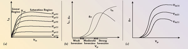
Fig. 1 Drain current and device transconductance versus gate voltage.
The transfer characteristics of the MOS transistor behave differently in different regions of the device operation. For example, the drain current in a weak-inversion region is mainly dominated by the diffusion component that increases exponentially with the gate voltage.3 On the other hand, in the strong-inversion region when the gate-source voltage Vgs is greater than the threshold voltage Vth, the drain current is proportional to the square of (Vgs–Vth). However, with a further increase of Vgs, the sensitivity of the drain current to the gate-source voltage increase becomes smaller. Therefore, to link all regions of the device operation with analytically derived closed-form expressions, it is necessary to use transcendental functions.2,4 As seen, the transconductance gm, derived by differentiating Ids, reaches a maximum and then decreases with increasing Vgs due to the influence of Vgs on the effective carrier mobility and the increasing effect of the series parasitic resistances with increasing Ids. For lower drain-sources voltages, Vds(1) < Vds(2) < Vds(3), the maximum value of the transconductance gm is reduced, with the corresponding significant degradation of the transconductance at large gate bias voltages.5 This means that the closer the drain bias voltage is to the saturation region, the faster the reduction in ?Ids for the same ?Vgs at large gate-source bias voltages Vgs.
It is necessary, however, to distinguish the device DC operation regions from its operation regions under the the RF signal. Generally, the large-signal transistor behavior is divided into three operation regions, as shown in Figure 2.6 The region where the input driving voltage vgs is less than the threshold voltage Vth, that is vgs £ Vth, is called the pinch-off or cut-off region. The term pinch-off is normally used for FET devices. The operation region, where vgs> Vth, is called the active or linear region, where the transistor can be considered as a voltage-controlled current source responding linearly to the gate voltage drive. Finally, the transistor is roughly equivalent to a resistance Rsat, operating in the saturation region. Unlike a DC current saturation region, the RF saturation region corresponds to a voltage saturation, since there is a particular saturation voltage Vsat corresponding to a fixed load resistance and defined by the intersection point between the load line and linear part of the I-V curves. The saturation or on-resistance Rsat is defined as the slope of the linear part of the I-V curves, that is Rsat = dvds/dids.
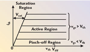
Fig. 2 Idealized transistor I-V characteristics showing the regions of RF operation.
In a class B operation mode with a piecewise-linear approximation of the transistor transfer characteristic, an active device operates both in the active and pinch-off regions. The magnitude of the output current exceeds a zero value during only half the entire signal period, representing a half-cosine waveform, as shown in Figure 3. In this case, because the parallel resonant LC circuit has a high quality factor, ideally only the fundamental frequency signal is flowing into the load, whereas the higher order harmonic frequency components are short-circuited.
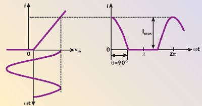
Fig. 3 Output current waveform for a device operating in class B.
Analytically such an operation can be written as

where
Iq = quiescent current
I = output current amplitude
? = half the conduction angle, indicating the part of the RF current cycle for which device conduction occurs and determines the moment when the output current i takes a zero value
At this moment,
![]()
and ? can be calculated from

Consequently, in a common case,

When ?t = 0, the output collector current has a maximum amplitude of
From Equation 3, the basic definitions can be derived as
when ? > 90°, then cos? < 0,Iq > 0
corresponding to class AB operation
when ? = 90°, then cos? = 0,Iq = 0
corresponding to class B operation
when ? < 90°, then cos? > 0,Iq < 0
corresponding to class C operation
As a result, the periodic half-cosine output current i can be represented as a Fourier series expansion:
![]()
The DC, fundamental and higher order harmonic frequency components can be obtained from


where

are the DC, fundamental and nth harmonic current coefficients, respectively.
It should be noted that, in an ideal class B with ? = 90°, the current coefficients for the third and higher order odd harmonics are equal to zero. Consequently, a half-cosine waveform consists of the DC and even-order harmonics only. In a real situation, when the transistor transfer characteristic has a quadratic dependence at its initial part, the output current waveform slightly deviates from an ideal waveform.
In an active region, the cosine voltage amplitude across the tank resistance RL, connected in parallel to the tank circuit, can be written using Equations 7 and 8 as

which is a linear function of the DC current components for a fixed conduction angle and tank resistance. However, for a varying conduction angle, being defined by bias conditions and voltage drop across the current source, the voltage amplitude is a function of ?. For example, the voltage amplitude will be higher by p/2 in class B with ? = 90°, compared with an idealized non-harmonic condition of class A with ? = 180°. Using the tank loaded Q, QL = w0CRL, where w0 = 1/Œ„„„LC is the oscillation frequency, Equation 10 can be rewritten as

showing the voltage amplitude reduction with the degradation of the loaded Q factor. This happens when the voltage amplitude V approaches the saturation region with an increasing shunting effect of the drain-source resistance, reducing the value of Rsat. In this case, the voltage waveform across the tank resistance cannot be considered to be purely cosinusoidal because of the significant harmonic contribution. Consequently, any consideration of the voltage amplitude as constant in a saturation region, introduced by Ham and Hajimiri,7 can only be applied as a first-order approximation, since the contribution of the fundamental voltage spectral component will depend on the overall voltage waveform, which will be different for different load and bias conditions.
Now let us consider a class B operation with increased amplitude of the cosine voltage across the tank, using the transistor I-V curves. In this case, as it follows from Figure 4, an active device operates in saturation, with active and pinch-off regions, and the load line follows a broken line LKMP with three linear sections (LK, KM and MP).2 The new section LK corresponds to the saturation region, resulting in the half-cosine current waveform with a depression in the top part. With further increase of the voltage amplitude, the output current pulse can be split into two symmetrical pulses containing a significant level of the higher order harmonic components. Similar simulated drain waveforms of a 1.8 GHz differential oscillator, based on a 0.18 mm CMOS process and operating simultaneously in the pinch-off, active and saturation regions, are given in Hajimiri and Lee.8

Fig. 4 Collector voltage and current waveforms for a device operating in saturation with active and pinch-off regions.
Start-up and Steady-state Conditions
The determination of the start-up and steady-state oscillation conditions is very often based upon a loop or nodal analysis of the circuit. However, the oscillator analysis using matrix techniques brings out the similarities between several types of oscillators and results in one group of equations, which can be used to analyze the different oscillator configurations.9 In this case, a two-port network can represent both the active device and feedback element. Depending on the oscillator configuration, in the form of a parallel feedback or a negative resistance (conductance), an oscillator with parallel or series feedback using admittance Y- or impedance Z-parameters, can be respectively modeled.
Three basic oscillator schematics are shown in Figure 5. For the basic representation of a single frequency negative conductance oscillator (a), the steady-state oscillation condition can generally be expressed through Y-parameters as

where

is the output admittance expressed through the Y-parameters of a loaded two-port network, which includes the device and feedback elements.

Fig. 5 Basic oscillator schematics.
The generic schematic of the modified Colpitts oscillator (b), with a parallel resonant circuit, is called a Seiler oscillator.10 Here, C2 and C3 represent the feedback capacitors and RL is the load resistor, which generally can include any losses in the tank inductor L. Such an oscillator configuration is useful for wideband frequency tuning when the capacitance C1 in the tank circuit is variable. Note that grounding of any terminal of the oscillator circuit does not change its electrical performance provided there are no changes in the connection of the feedback elements and load to the active device. To analyse the oscillator start-up and steady-state conditions, it is convenient to consider a common gate configuration of this circuit, since the load resistance is connected between the drain and gate terminals. In this case, the common gate admittance matrix [Y]CG for a two-port network expressed through the common source Y-parameters can be written as

where Yij (i,j = 1,2) are the common source Y-parameters.2
Then, a steady-state oscillation condition for the oscillator circuit (c) can be rewritten through the device common source Y-parameters and feedback admittance Y2 = j?C2 and Y3 = j?C3 as
![]()
where

Separate equations for real and imaginary parts of the output and load admittances of a negative conductance oscillator can be obtained from Equation 15:

Similarly, the start-up conditions for a negative conductance oscillator are written as

To obtain the explicit analytical relationships between the active device and resonant circuit parameters, consider the simplified intrinsic MOSFET high frequency equivalent circuit shown in Figure 6, where Cgs is the gate-source capacitance, gm is the transconductance and Cds is the drain-source capacitance. The admittance Y-parameters of the equivalent circuit are

Substituting the device Y-parameters into Equation 16 allows the real and imaginary part of the output admittance to be represented through the elements of the device parameters as

From Equations 23 and 24, it follows that, in a common gate configuration, the real part of the output admittance is negative and the imaginary part of the output admittance has a capacitive reactance. At frequencies w << ?T, where ?T = 2?fT, fT = gm/2?Cgs is the device transition frequency, Equation 23 can be simplified to
Substituting Equations 25 and 24 into Equations 20 and 21, representing the oscillator start-up conditions, yields


Fig. 6 Simplified MOSFET equivalent circuit.
From Equation 26, it follows that the build-up of the self-oscillations will be more easily provided at lower frequencies, higher ratio of Cgs/Cds and smaller losses in the circuit. In addition, the regeneration factor or start-up margin can be improved by selecting the proper values of the external feedback capacitances C2 and C3 connected between the gate-source and drain-source terminals in parallel to the gate-source and drain-source capacitances Cgs and Cds, respectively. As it follows from Equation 27, the oscillation frequency is a function of not only the external reactive elements but also the device parameters.
In a steady-state mode, the device small-signal transconductance should be considered as fundamentally averaged during the large-signal operation. By using a piecewise-linear approximation, its large-signal definition can be written as gm?l(?). Thus, assuming constant capacitances Cgs and Cds whose values are given by the operating DC bias point, the oscillator steady-state conditions can be rewritten as

where gm and ?T are the small-signal transconductance and angular transition frequency, respectively. The value of the small-signal gate-source capacitance Cgs is equal to the oxide capacitance at low and high bias voltages, and is reduced by approximately two to three times in a region near the threshold voltage. The drain-source capacitance Cds can be considered as the junction capacitance, for which the maximum large-signal value deviates from the small-signal value by not more than 10 to 20 percent.2 Consequently, as a first-order approximation, the capacitances Cgs and Cds can be modeled as the fixed capacitances measured at the quiescent bias voltage.
Differential Cross-coupled Oscillator
It is most convenient to describe the operational principle of the differential cross-coupled LC oscillator on the example of an ideal class B operation with a piecewise-linear approximation of each transistor transfer characteristic, which means that each transistor conducts exactly half a 180° cycle with zero quiescent current. The simplified equivalent circuit of the differential cross-coupled LC oscillator with the tail current source is shown in Figure 7. If the quality factor of the tank circuit is assumed sufficiently high to provide the sinusoidal voltages applied to the gate-source terminals of the transistors and across the tank resistor RL, the drain current of each transistor can be represented in the following half-sinusoidal form.
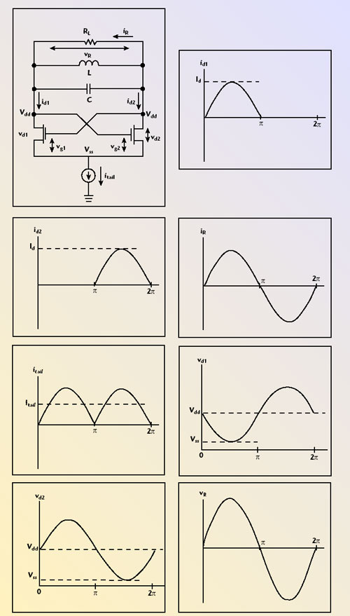
Fig. 7 Differential cross-coupled LC oscillator circuit schematic and operation principle.
For the first transistor:
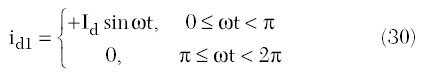
For the second transistor:
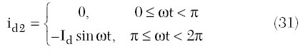
Since, for an idealized piecewise-linear approximation, the third and high order odd harmonics of the drain currents are equal to zero, the total iR flowing across the tank resistor RL is the difference of the two out-of-phase drain currents:
![]()
representing a purely sinusoidal waveform.
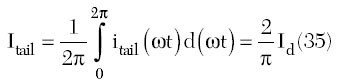
The current flowing into the tail current source through the center point of the circuit is the sum of the drain currents:

containing the DC and even-order harmonic components.
Ideally, even-order harmonics are cancelled out and should not appear at the resistor. In practice, the second harmonic is suppressed by approximately 20 dB or more below the fundamental. It is necessary to connect a bypass capacitor to the center point of the circuit in order to exclude power losses due to even-order harmonics. The current iL produces a sinusoidal voltage across the resistor RL equal to
![]()
The DC component Itail of the total drain current itail can be defined by integration over the oscillation period as
Conclusion
The basic principles of the active device operation regions under DC and RF large-signal modes, based upon using CMOS devices, are presented with the derivation of very simple analytical voltage-current relationships. By using a matrix technique, an analysis of the start-up and steady-state oscillation conditions can be significantly simplified, resulting in explicit analytical dependences between the device and feedback parameters. These conditions are derived for a widely used single-ended MOSFET oscillator with a parallel resonant circuit based on a simplified device equivalent model. The basic operation principle of a differential cross-coupled tail-biased oscillator is explained analytically in the time domain.
References
1. R.S. Muller and T.I. Kamins, Device Electronics for Integrated Circuits, John Wiley & Sons Inc., New York, NY, 1977.
2. A. Grebennikov, RF and Microwave Power Amplifier Design, McGraw-Hill, New York, NY, 2004.
3. Y.P. Tsividis, Operation and Modeling of the MOS Transistor, McGraw-Hill, New York, NY, 1987.
4. M. Bucher, C. Lallement and C.C. Enz, “An Efficient Parameter Extraction Methodology for the EKV MOST Model,” Proceedings of the 1996 IEEE International Conference on Microelectronic Test Structures, pp. 145–150.
5. M.C. Ho, K. Green, R. Culbertson, J.Y. Yang, D. Ladwig and P. Ehnis, “A Physical Large-signal Si MOSFET Model for RF Circuit Design,” 1997 IEEE MTT-S International Microwave Symposium Digest, pp. 391–394.
6. H.L. Krauss, C.W. Bostian and F.H. Raab, Solid State Radio Engineering, John Wiley & Sons Inc., New York, NY, 1980.
7. D. Ham and A. Hajimiri, “Concepts and Methods in Optimization of Integrated LC VCOs,” IEEE Journal of Solid-State Circuits, Vol. SC-36, June 2001, pp. 896–909.
8. A. Hajimiri and T.H. Lee, “Design Issues in CMOS LC Oscillators,” IEEE Journal of Solid-State Circuits, Vol. SC-34, May 1999, pp. 717–724.
9. A.J. Cote, “Matrix Analysis of Oscillators and Transistor Applications,” IRE Transactions on Circuit Theory, Vol. CT-5, September 1958, pp. 181–188.
10. J.K. Clapp, “Frequency Stable LC Oscillators,” Proceedings of the IRE, Vol. 42, August 1954, pp. 1295–1300.
Andrei Grebennikov received his MSc degree in electronics from the Moscow Institute of Physics and his PhD degree in radio engineering from the Moscow Technical University of Communications and Informatics in 1980 and 1991, respectively. He joined the scientific and research department of the Moscow Technical University of Communications and Informatics as a research assistant in 1983. From 1998 to 2001, he was a member of the technical staff at the Institute of Microelectronics, Singapore, responsible for the design and development of LDMOS FET high power amplifier modules. Since January 2001, he has been with MA/COM Eurotec as a principal engineer, where he is involved in the design and development of the handset advanced transmitter architectures in general and in GaP/GaAs HBT power amplifier modules for new generations of wireless communications systems. His scientific and research interests include the design and development of power RF and microwave radio transmitters for base station and handset applications, hybrid integrated circuits and MMIC of high efficiency, and linear microwave and RF power amplifiers, single-frequency and voltage-controlled oscillators using any type of bipolar and field-effect transistors, and active device modeling.