
The speed to market is critical to the success of any RFIC company. With more and more wireless standards proposed and adopted, the design cycles are actually getting shorter. It puts a lot of pressure on the RFIC team to come up with the design faster. In the digital CMOS design, the basic building blocks can be scaled based on the process. In RFIC CMOS design, each transceiver has to be tailored to the specific application because RFIC is heavily frequency dependent. Even though the new RFIC cannot simply be scaled down as the digital IC, the basic topologies can be reused extensively. After examining hundreds of transceiver RFICs and their building blocks, it is easy to see what the dominant topology is for each building block in a typical RFIC. In this article, the most widely used topologies of each building block are presented. Those building blocks can be the starting point for any generic RFIC design. They need to be optimized for the specific application. For example, the matching circuits need to be designed according to the frequency, even though the topology is the same.
A generic wireless transceiver consists of three main blocks: a transmitter (TX), a receiver (RX) and a synthesizer. The major building blocks in a direct conversion TX are a baseband filter, a modulator, the RF filter, an automatic gain control (AGC) circuit, a power amplifier (PA) and the power detector loop. The modulator (MOD), the AGC and the PA are discussed extensively in this article. A direct conversion RX normally consists of a RF SAW, a low noise amplifier (LNA), an image rejection SAW, a demodulator (DEMOD), an AGC and a RX baseband filter. The DEMOD and the AGC topology in a RX are similar to the ones used in a TX with minimal modifications. They will be covered in the TX MOD and AGC discussion. The synthesizer is typically made up of a voltage-controlled oscillator (VCO), a phase/frequency detector (PFD), a charge pump (CP), a frequency divider and a digital logic control block. For the synthesizer discussion, all but the digital logic control will be discussed.
This article starts with the discussion on the LNA. The PA is next. The MOD/DEMOD and the AGC discussion are shared for a TX/RX. The article ends with the discussion on the synthesizer.

The LNA’s performance directly impacts the receiver performance, especially the RX sensitivity. Gain, noise figure (NF), input third-order intercept (IIP3), stability and I/O matching are important design parameters. It is difficult to achieve the best performance in one parameter without sacrificing another. The classical tradeoff is gain versus NF. A single-ended and a differential version of the popular LNA designs are shown in Figure 1. The Miller effect increases the parasitic capacitance at the gate of the LNA. A cascode topology reduces this effect by stacking a common gate (CG) stage on a common source (CS) gain stage. The input and output port are better isolated to reduce the parasitic capacitance between the gate and drain. In the single-ended version, M1 is the CS stage while M2 is the CG stage. L1 is the degenerated feedback element to bring the input NF circle and the gain circle closer. Thus, a compromise between NF and gain can be reached. L3 is the input matching element. C1 is the input DC block. The LNA is biased in a current mirror configuration with M3, I1 and R1. In a highly integrated IC circuit, the common mode noise is a major problem. A differential circuit is often used to combat this problem. The differential LNA can be considered as two single-ended LNAs with the tail bias current. The tail current out of M7 is important to reduce the common mode noise. Without it, there will not be enough common mode degenerated resistance to reduce the common mode noise. The bias current is set by the current mirror consisting of M6 and M7. It, in turn, sets the Vgs of M1 and M2. The drain voltage of M7 is set by the current mirror biasing at the gate of the M1 and M2.

The PA is the next block on deck. The CMOS PA has gradually replaced the HBT or GaAs FET in the low to medium power applications like Bluetooth, WLAN, etc. Its performance is inferior, compared to the HBT or the GaAs FET, but the CMOS PA can be easily and cheaply integrated in the CMOS transceiver. Many design imperfections can be corrected by the baseband digital processor.
The PA design is similar to a LNA or a general-purpose gain block, but its emphasis is on output power, linearity and efficiency. The design starts at the output port where the output power contours of the device are characterized. Once the output termination is determined, the matching circuit is designed the same waay as the other RF building block’s matching circuits. A two-stage common source FET with RC feedback is shown in Figure 2. M1 and M2 are the driver stages. M3 and M4 are the output power stage. The RC feedback from the drain to the gate stabilizes the transistors at the high frequency. The feedback also broadens the bandwidth of the PA. M5 and M6 and M7 and M8 are the active resistive dividers to bias the driver stage and the power stage, respectively. The cascade PA design is popular as well. Topology wise, it is similar to the cascode LNA. M1 through M4 are the driver stage, while M5 to M8 complete the power stage. An integrated balun is utilized in this design since the most widely used antennas in wireless devices are single ended.
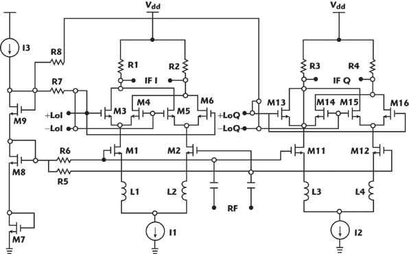
The DEMOD is used to convert an RF signal to baseband in a direct conversion receiver or to a low IF signal in a Very Low IF (VLIF) RX. Since most modern wireless devices require both I and Q channels, two double-balanced mixers (DBM) are needed in the DEMOD. The implementation is illustrated in Figure 3. M1 to M6 is the DBM for the I channel. M11 to M16 is the DBM for the Q channel. Since the same DBM is used for both I and Q channels, only one DBM is discussed in detail. The incoming RF signal is amplified first by the gain stage such as M1 and M2. M3 to M6 are the switching FETs. It fundamentally serves the purpose of a multiply operation. In half the cycle, M3 and M6 are on. The local oscillator (LO) and RF are essentially multiplied in phase. In the other half of the cycle, M4 and M5 are turned on to reverse the polarity of the output signal. The output loads are implemented with resistors R1 to R4. The degenerated feedback inductors L1 to L4 help the IIP3 performance. The biasing is done with the diode connected FETs. The MOD’s topology is similar to the DEMOD. The RF and IF positions need to be swapped. The signal-combining network needs to be swapped as well.
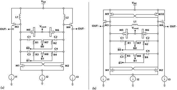
The same AGC circuit can be used in either a TX or a RX. There are many AGC topologies to choose from. The variable transconductance and the variable biasing AGC are the most popular for the high frequency operation. They are shown in Figure 4. The variable transconductance circuit is based on the principle that the transconductance of the FET changes as the FET goes from a saturation mode to a triode mode. Thus, the gain is varied. M1 to M4 can be considered as the typical differential cascode gain stage. The difference is that Vcont is applied at the gates of M3 and M4. As Vcont decreases, the drain voltage at M1 and M2 drops. Eventually M1 and M2 enter the triode region. M7 to M10 are the current source type load. Thus, a common mode feedback (CMFB) is needed to make sure the current source matches with the current sink I1.

The common mode voltage is sampled at the drain of M3 and M4 with M5 and M6. M5 and M6 can be considered as two large value resistors. They have the same value. The sampled voltage is fed to a comparator (M11 to M14). The reference is fed to one input M14, while the sampled common mode is fed to the other input M13. The error voltage is used to control the bias current out of the current source M8 and M9. M8 and M9 are the current bleeding path. The closed feedback loop ensures correct bias current follows with the desired reference voltage.
The variable current AGC is based on the idea that the tranconductance of a FET changes with the bias current. By varying the bias current in the FET, the AGC can be accomplished. M1 and M2 are the input gain buffer. M4 and M5 are the current bleeding path. If Vcont is larger than the Vref, more bias current flows through M3 and M6. In this mode, a high gain is expected. When Vcont is reduced, more bias current flows through M4 and M5, and the gain is thus reduced. M7 and M8 are the output emitter follower buffers to reduce the output impedance. R1 is the degenerated resistor to improve the linearity of the AGC.
The CMOS VCO is based on the negative resistance theory. Two approaches are shown in Figure 5. In the NMOS only version, by cross coupling M1 and M2, a positive feedback is created in the circuit. Looking into the gate of M1 and M2, a negative resistance can be expected. The operating frequency is set by the tank circuit resonance. L1 and L2 provide the inductance part. The frequency can be tuned coarsely by the capacitance banks and fine-tuned with the varactor capacitors. In the circuit shown, two-bit, four-state capacitance banks are used. More banks can be added if a larger process variation is expected. By turning M7 and M8 on and off, more or less total capacitance can be expected in the resonator tank. The varactor is implemented with the FETs M5 and M6 by tying the source and drain. M3 and M4 are the output buffers.
In the complementary CMOS VCO, the key change is to add a cross-coupled PMOS pair. By adding a PMOS pair, two more elements are added to contribute to the negative resistance while the bias current remains the same. It is more power efficient.
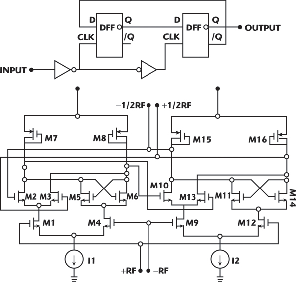
The high-speed frequency divider or a prescaler are typically implemented with a Johnson counter or a divide-by-two building block. Its block diagram and detailed implementation are shown in Figure 6. The Johnson counter consists of a master DFF (D-type flip-flop), a slave DFF and a couple of inverters. In 50 percent of the input duty cycle, the master DFF is on. For the rest of the 50 percent duty cycle, the slave DFF is on. The divided-by-two outputs are taken from the outputs of both DFF. The outputs are 90° phase shifted by the nature of the Johnson counter. Since the master and slave DFFs are identical, only the master DFF is discussed in detail. A DFF is based on the emitter-coupled logic. This logic works by steering the bias current. Thus, it is a faster logic compared to the CMOS logic. M1 and M4 are the input buffer. M5 and M6 are the latch element. M2 and M3 can be considered as the mode switch to decide to load a new input value or to keep the current value. M7 and M8 are the diode tied load. A resistor load can be used as well.
The charge pump is used in the synthesizer to source or sink current from the external loop filter. The basic idea is to add a switch in both the current source and current sink paths. The switch can be added at the gate, source or drain, as shown in Figure 7. To reduce the effect of the charge sharing, clock feed-through and charge injection, switching at the source is the best choice because the switch is relatively isolated from the output. Icp is the reference current for both the current sink and the current source. For the current sink path, Icp is mirrored into the M6 and M5 path through the modified stacked current mirror (M1, M2, M5 and M6). The advantage of this current mirror is the low supply voltage requirement. M15 is the source switch for the current sink. M13 is a dummy FET to ensure that M1 and M5 have the same DC source voltage. For the current source path, Icp is first mirrored by a modified stacked current mirror (M1, M2, M3 and M4). Then it is mirrored again by the PMOS current mirror (M7, M8, M9 and M10). M11 is the switch for the current source.
To reduce the mismatch problem and to increase the speed of the CP, a current steering CP is often used. The switches are implemented with a current steering pair (M1 and M2, M3 and M4). Icp is mirrored to the current steering pair via the modified stacked current mirror. To source the current, UP is logic H and /UP is logic low. Icp goes through the path of M1 and then it reaches the output via another current mirror (M5 and M6). To sink the current, the DOWN control pair is activated. Because the current is steered instead of charging/discharging, it will be faster than the switching at the source approach. However, it will burn more power since the current path is not really shut off when it is not used.

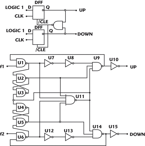
The UP/DOWN control signals used in CP are generated by the PFD. The two DFFs implementation has been a workhorse for a long time. Its block diagram and the circuit implementation are shown in Figure 8. The upper and lower DFFs generate UP and DOWN signals, respectively. When f1 arrives first at the upper DFF, the UP signal is generated to turn on the current source. When f2 arrives at the the lower DFF, its output is logic H. When both UP and DOWN are logic H, NAND gate resets both DFFs to output logic L. Thus, the phase difference between the two signals are detected and used to turn on either the current sink or current source of the CP.
Each major building block in a modern wireless transceiver is discussed in this article. The circuits are generic enough to be adopted in most wireless applications. It will be offered as a good starting point for the next RFIC design. For an RFIC company, a modular RFIC standard cell approach will shorten the design cycle and reduce the design risks. For a foundry company, a portfolio of RFIC IPs will add more value to its customers. The RFIC designs no longer need to start with a blank paper. The modular standard cell approach will make future RFIC designs easier to tackle.
References
1. B. Razavi, RF Microelectronics, Prentice-Hall, Upper Saddle River, NJ, 1998.
2. R.L. Geiger, P.E. Allen and N.R. Strader, VLSI Design Techniques for Analog and Digital Circuits, McGraw-Hill, New York, NY, 1990.
3. B. Razavi, Design of Analog CMOS Integrated Circuits, McGraw-Hill, New York, NY, 2001.
4. T.H. Lee, The Design of CMOS Radio-frequency Integrated Circuits, Cambridge University Press, New York, NY, 2004.
5. J.P. Uyemura, Introduction to VLSI Circuits and Systems, John Wiley & Sons Inc., Hoboken, NJ, 2002.
6. S.C. Cripps, RF Power Amplifier for Wireless Communication, Artech House Inc., Norwood, MA, 1999.
7. G. Gonzalez, Microwave Transistor Amplifiers Analysis and Design, Prentice-Hall, Upper Saddle River, NJ, 1997.
8. M.H. Perrott, High Speed Communication Circuit and Systems, MIT OCW, Cambridge, MA, 2003.
9. H.L. Krauss, C.W. Bostian and F.H. Raab, Solid State Radio Engineering, John Wiley & Sons Inc., Hoboken, NJ, 1980.
10. A. Podell, “RFIC Design and Applications,” Besser Associates.
11. J. Young, “RF CMOS Design,” Besser Associates.
12. J.W. Rogers, Radio Frequency Integrated Circuit Design, Artech House Inc., Norwood, MA, 2003.
13. U.L. Rohde and D.P. Newkirk, RF/Microwave Circuit Design for Wireless Applications, John Wiley & Sons Inc., Hoboken, NJ, 2000.
14. J. Crols and M. Steyaert, CMOS Wireless Transceiver Design, Kluwer Academic Publishers, 2003.
15. L. Fan Fei, “Subharmonic Mixer IC Designs and Enhancement Techniques,” Microwave Journal, Vol. 48, No. 9, September 2005, pp. 214–218.
16. L. Fan Fei, “Frequency Divider Design Strategies,” RF Design, March 2005.
17. L. Fan Fei, “CMOS Oscillator Design Considerations,” Microwave Journal, Vol. 50, No. 4, April 2007, pp. 136–142.
18. L. Fan Fei, “Enhance CMOS Charge Pumps and Phase-frequency-detectors,” Microwaves & RF, September 2007.
19. L. Fan Fei, “CMOS Power Amplifier Design Strategies,” Microwaves & RF, November 2007.
20. L. Fan Fei, “CMOS AGC Design Strategies,” Microwave Journal , Vol. 51, No. 2, February 2008, pp. 156–162.
21. L. Fan Fei, “Integrated Power Detector Solutions and Design Strategies,” www.rfdesignline.com, October 3, 2007.

Louis Fan Fei received his BEE and MSEE degrees from Georgia Tech in 1996 and 1998, respectively. He worked on microwave instrument circuits for HP/Agilent in Colorado Springs, CO, in the summer of 1997 and on WLAN and wireless local loop circuits at Lucent/Agere Systems from 1998 to 2003. He is now an RF engineer at Garmin International, where he designs GPS receivers.