
In modern digital wireless communication systems, such as IS-95, PCS, W-CDMA, OFDM and so on, power amplifiers have progressed towards having a wide bandwidth and a large number of carriers. Recently, orthogonal frequency division multiplexing (OFDM) modulation has become an attractive technique for transmitting information efficiently within a limited bandwidth like WiBRO and WiMAX. However, since the OFDM signal consists of a number of independently modulated sub-carriers, it produces a higher peak-to-average power ratio (PAR) signal. A typical PAR for a 64-subcarrier OFDM signal is approximately 8 to 13 dB. When the number of sub-carriers is increased to 2048, the PAR is also increased to 11 to 16 dB. The available efficiency of the power amplifiers designed for these high PARs will be significantly deteriorated.
The Doherty amplifier is known as a technique for improving the efficiency at high output back-off power. Its primary advantage is the ease of configuration when applied to high power amplifiers, unlike other efficiency enhancement amplifiers or techniques such as switching mode amplifiers, EER, LINC and so on.1 Recent results have been reported on its use as a symmetric Doherty structure,2 an asymmetric Doherty structure with uneven power transistors3 and as an N-way Doherty structure using multi-paralleled transistors.4 In the case of the symmetric Doherty amplifier, the maximum efficiency point is obtained at a 6 dB back-off power. The asymmetric Doherty amplifier can obtain a high efficiency at various back-off powers using a combination of uneven power device sizes for the main and peaking amplifier.
Unfortunately, it is difficult to optimize the gain and output power of the asymmetric Doherty amplifier because of the different device matching circuits and the delay mismatch between the main and peaking amplifier. The conventional N-way Doherty amplifier has an efficiency enhancement over a conventional two-way Doherty structure by using multiple parallel transistors of identical devices. Its one drawback is that the total gain will be reduced due to the loss of the N-way input power splitter. Under low gain situations, this will increase the power dissipation of the driving amplifier.
In order to prevent the total gain of the Doherty amplifier from degrading, the peaking amplifier is designed using a dual-fed distributed amplifier structure. Distributed amplification is a technique whereby the power combining is performed directly at the transistor level without the need for an N-way power combiner.5 Therefore, it is an easy configuration for combining peaking amplifiers.
Operational Principles of an N-way Distributed Doherty Power Amplifier
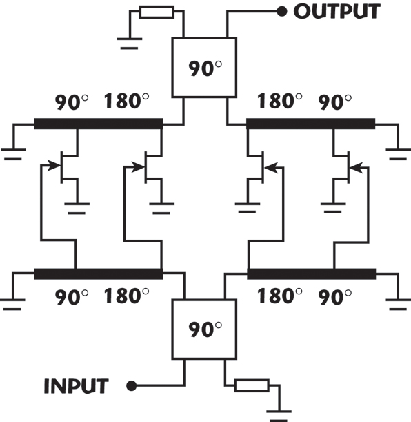
The distributed power amplifier, which was described by Eccleston,5 is a simple and feasible way to increase the gain performance of a power amplifier. The balanced dual-fed distributed amplifier approach shown in Figure 1 can be formed by using a pair of identical single-ended distributed power amplifiers and quarter-wave hybrid couplers. As viewed on the single-ended distributed structures, a hybrid is used to feed both ends of the gate lines and another hybrid combines the waves appearing at the ends of the drain lines, thereby increasing the gain. The FET drain voltages and currents are equal when the FETs are spaced by a half-wavelength at the center frequency when using an input and output power splitter/combiner and an even number of FETs.
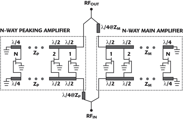
Figure 2 is the schematic of a new N-way distributed Doherty power amplifier, based on a distributed structure. The distributed Doherty amplification approach uses a power combiner and a splitter at the output and the input, respectively. This will improve the isolation between the main amplifier and the peaking amplifier. Both the N-main amplifiers and N-peaking amplifiers are combined using half-wave and quarter-wave microstrip lines.
In order to understand the load impedance variation of the N-way Doherty amplifier, it can be analyzed by the equivalent conversion of AC multi-current sources. Figure 3 shows the operational principle of load modulation for the N-way distributed Doherty power amplifier. Im,M and Ip,P are ideal AC current sources for the carrier amplifiers and peaking amplifiers, respectively. The –90° phase difference between the main source and the peaking source is selected to compensate for the phase shift by the quarter-wave transformer, which is necessary to the Doherty operation. The output node voltage, V0, through the load resistor, R0/(M+P), can be given by

Thus, the impedance of the main amplifier, which can be seen from the quarter-wave transformer, Z'm, can be writtem as

Then, assuming that IM and IP are MIm and PIp, respectively, the impedance of the main amplifier, which can be seen from the main current souce, Zm, can be found by

If identical devices are used in the main and peaking amplifiers, the load impedance of an N-way Doherty amplifier could be modulated as a function of the number of N-ways. Finally, the load impedance of the N-way Doherty amplifier as a function of three operational regions of the peaking amplifier could be divided by:
• When Ip is 0, the load impedance becomes (1+P/M) Ro.
• When Ip is equal to Im, the load impedance becomes Ro.
• When Ip is smaller than Im, the load impedance transits from N* Ro to Ro.
The efficiency of an N-way Doherty amplifier, which is comprised of M, class B biased, main amplifiers and P, class B biased, peaking amplifiers, can also be divided into three input power regions (low, medium and peak levels).4

where
νo = output voltage for a given power level
νmax = maximum output voltage for a given power level
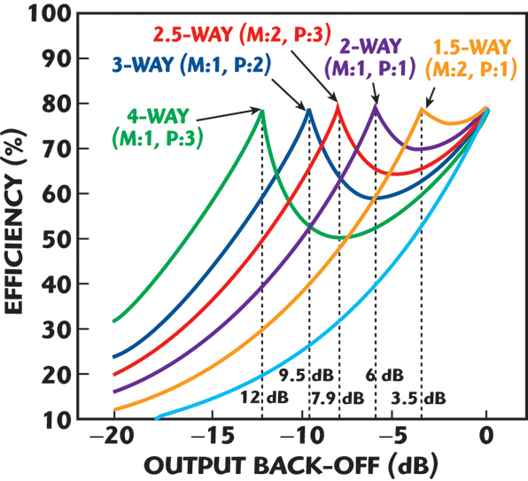
Figure 4 shows the calculated efficiency of the N-way Doherty amplifier, for different topologies, at various back-off powers: 3.5, 7.9, 9.5 and 12 dB. The desired location of the peaking point of an N-way Doherty amplifier can be easily derived from Equation 4. This peaking point is defined as the extended back-off state, XBO, and is given

where
P = number of peaking amplifiers
M = number of main amplifiers

The schematic of the proposed three-way distributed Doherty amplifier is shown in Figure 5. In order to provide high efficiency at a back-off power of 9.5 dB, two peaking amplifiers are combined using the dual-fed distributed structure. It consists of half-wave and short-circuited quarter-wavelength microstrip lines. This structure should insure that the total gain of the N-way distributed Doherty amplifier should not be degraded compared to the conventional N-way Doherty amplifier.
Design and Simulation
The proposed three-way distributed Doherty amplifier design uses the same device for the one main amplifier and the two peaking amplifiers. The main amplifier is biased in the class AB mode and the peaking amplifiers are biased in the class C mode. The devices are Freescale high power MRF21045 LDMOS FETs with a peak envelope power (PEP) of 45 W. The simulation for the Doherty circuit was performed using Agilent’s ADS software.
Optimization of the N-way distributed Doherty amplifier required the following:
• Evaluating the optimum number of main amplifiers (M) and peaking amplifiers (P) for the given back-off power
• Bias adjustment of the main amplifier in class AB mode

• Gate bias adjustment of the peaking amplifiers in class C mode
• Offset line optimization for achieving a peaking point at the desired back-off power
The shunt capacitors, CP, are inserted so that both gain and efficiency of the Doherty amplifier are optimized. The other shunt capacitor, CM, is also used for optimizing the linearity.6
Figure 6 shows the simulated PAE and gain performance of the proposed three-way distributed Doherty amplifier using a single tone at 2140 MHz. The operating point of the class AB biased main amplifier is: IDQ = 510 mA, VGS = 3.82 V and VDS = 27 V. The operating points of the class C biased peaking amplifiers are:
Peaking amplifier 1:
IDQ = 0 mA, VGS = 2.4 V and VDSc = 27 V.

Peaking amplifier 2:
IDQ = 0 mA, VGS = 2.6 V and VDS = 27 V.
The output impedance of the combined peaking amplifier using a dual-fed distributed structure was (4.65+j 2.1)Ω. The offset line is necessary to prevent leakage power between the main amplifier and the peaking amplifier. An offset line of approximately 0.25 λ was inserted; this corresponds to an optimum output resistance of 521 Ω. From the simulated results, a 43 percent PAE was obtained at a PEP of approximately 200 W. Consequently, a 40 percent PAE at 9.5 dB back-off power from the peak efficiency point was achieved. This was an efficiency improvement of approximately 7 percent compared to that of the two-way conventional Doherty amplifier at a 6 dB peaking point. A gain of approximately 10.5 dB was obtained from 2130 to 2150 MHz. This was similar to that of the conventional two-way Doherty amplifier.
Fabrication and Measurements
A new three-way distributed Doherty amplifier using Freescale’s MRF21045 was fabricated and measured at a center frequency of 2140 MHz and a single carrier W-CDMA signal with a peak-to-average ratio of 9.8 dB. Figure 7 is a photograph of the three-way distributed Doherty power amplifier. Figure 8 shows the measured PAE and gain performance of the proposed three-way distributed Doherty amplifier, using a single-tone, 2140 MHz signal. The main amplifier’s operating point is: IDQ= 480 mA, VGS= 3.9 V. The operating points of the peaking amplifiers are:
Peaking amplifier 1:
IDQ = 0 mA, VGS = 2.1 V.
Peaking amplifier 2:
IDQ = 0 mA, VGS = 1.9 V.
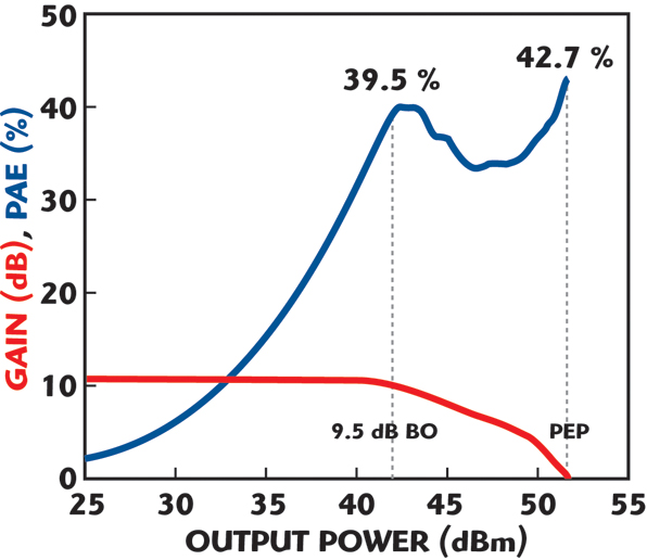
Shunt capacitors, CP = 15 pF and CM = 0.5 pF, are used. A 42.7 percent PAE at a PEP of 131 W and a 39.5 percent PAE at 9.5 dB back-off are achieved. A gain of approximately 11 dB was obtained at 9.5 dB back-off.
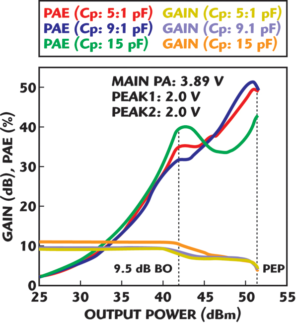
Figure 9 shows the measured PAE and gain as a function of the shunt capacitor CP values of 5.1, 9.1 and 15 pF, in order to find the optimal capacitance that could affect the gain and PAE of the Doherty amplifier. It was tested with a single-tone, 2140 MHz signal and the gate biases of the main amplifier and peaking amplifiers are fixed to 3.89 and 2.0 V, respectively.
Figure 10 shows the measured PAE and gain variations as a function of the shunt capacitor, CP, and the bias of the peaking amplifiers using a single-tone, 2140 MHz signal. Optimization of CP and of the bias point of the two peaking amplifiers produced efficiency and gain improvement of approximately 8 percent and 2 dB at 9.5 dB back-off, even though the PAE is reduced at PEP. Consequently, a high PAE of the distributed Doherty amplifier could be obtained by adjusting the shunt capacitor, CP, and the bias of the peaking amplifiers.

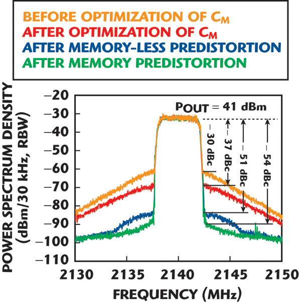
Figure 11 shows the measured W-CDMA, one-carrier spectrum of the three-way distributed Doherty amplifier before and after optimization of CM, and after digital predistortion. The test bench set-up of the digitally pre-distorted power amplifier and the operation principles have been published previously.8 After optimization of CM, a linearity improvement of 7 dB was achieved at a +2.5 MHz offset frequency. The operating points were VGS =3.79 V (Main PA), VGS = 3.1 V (Peaking PA1) and VGS = 2. 5 V (Peaking PA2). Shunt capacitors, CP = 9.1 pF and CM = 0.5 pF, were used. In order to achieve high linearity, both memory-less and memory-based digital predistortions were applied. The ACLR performance of –51 dBc after memory-less and –54 dBc after memory compensation were obtained at 41 dBm output power and +2.5 MHz offset frequency.
Table 1 shows the summary results of the proposed three-way distributed Doherty power amplifier. This research confirms that both high efficiency and high linearity for W-CDMA and OFDM power amplifiers can be achieved.
Conclusion
A novel Nth-way distributed Doherty amplifier was proposed to obtain high efficiency at various back-off power states. The peaking amplifiers of the N-way distributed Doherty amplifier were combined using a dual-fed distributed structure. From the measured results, the three-way distributed Doherty amplifier yielded a 39.5 percent PAE at 9.5 dB back-off power and a power gain of 11 dB. After final optimization for linearity and efficiency, –54 dBc ACPR and 33 percent PAE are achieved, using memory compensated digital predistortion.
Acknowledgment
This work was supported by the IT R&D program of MIC/IITA (2007-F-044-01, development of GaN power amplifier for 4G base station).
References

1. S.C. Cripps, RF Power Amplifier for Wireless Communications, Artech House Inc., Norwood, MA, 1999.
2. K.J. Cho, J.H. Kim and S.P. Stapleton, “A Highly Efficient Doherty Feedforward Linear Power Amplifier for W-CDMA Base Station Applications,” IEEE Transactions on Microwave Theory and Techniques, Vol. 53, No. 1, January 2005, pp. 292–300.
3. J.Y. Lee, J.Y. Kim, J.H. Kim, K.J. Cho and S.P. Stapleton, “A High Power Asymmetric Doherty Amplifier with Improved Linear Dynamic Range,” 2006 IEEE MTT-S International Microwave Symposium Digest, pp. 1348–1315.
4. Y. Yang, J. Cha, B. Shin and B. Kim, “A Fully Matched N-way Doherty Amplifier with Optimized Linearity,” IEEE Transactions on Microwave Theory and Techniques, Vol. 51, No. 3, March 2005, pp. 986–993.
5. K.W. Eccleston and O. Kyaw, “Analysis and Design of Class B Dual-fed Distributed Power Amplifier,” IEEE Proceedings on Microwave Antennas and Propagation, Vol. 151, No. 2, 2004, pp. 104–108.
6. K.J. Cho, W.J. Kim, J.H. Kim and S.P. Stapleton, “40 W Gallium-nitride Microwave Doherty Power Amplifier,” 2006 IEEE MTT-S International Microwave Symposium Digest, pp. 1387–1390.
7. M. Iwamoto, A. Williams, P. Chen, A.G. Metzger, L.E. Larson and P.M. Asbeck, “An Extended Doherty Amplifier with High Efficiency Over Wide Power Range,” IEEE Transactions on Microwave Theory and Techniques, Vol. 49, No. 12, December 2001, pp. 2472–2478.
8. K.J. Cho, W.J. Kim, S.P. Stapleton, J.H. Kim, J.Y. Kim, B. Lee, J.J. Choi and J.C. Lee, “An Enhanced Doherty Amplifier Design Based on the Derivative Superposition Method,” Microwave Journal, Vol. 50, No. 4, April 2007, pp. 72–89.

Kyoung-Joon Cho received his BS degree in information and communication engineering from Anyang University, Anyang, Korea, in 1998, and his MS and PhD degrees in radio science and engineering from Kwangwoon University, Seoul, Korea, in 2000 and 2004, respectively. He was a postdoctoral fellow in the school of engineering science at Simon Fraser University, British Columbia, Canada, from 2004 to 2007. He is currently a senior HPA designer at Dali Wireless, Sunnyvale, CA. His research interests include MMIC/hybrid high efficient power amplifier design and linearization techniques.

Wan-Jong Kim received his BS and MS degrees in radio science and engineering from Kwangwoon University, Seoul, Korea, in 1999 and 2001, respectively, and his PhD degree from the school of engineering science at Simon Fraser University, British Columbia, Canada, in 2006. Since 2007, he has been working as a senior DSP designer at Dali Wireless, Sunnyvale, CA. His research interests include peak-to-average power ratio reduction techniques, RF/DSP integrated system and digital linearization techniques.

Ji-Yeon Kim received her BS and MS degrees in radio science and engineering from Kwangwoon University, Seoul, Korea, in 2002 and 2004, respectively. She is currently working toward her PhD degree in radio science and engineering, Kwangwoon University, Seoul, Korea. Her research interests include high efficiency power amplifier design and linearization techniques.

Jong-Heon Kim received his BS degree in electronic communication engineering from Kwangwoon University, Seoul, Korea, in 1984, his MS degree in electronic engineering from Ruhr University, Bochum, Germany, in 1990, and his PhD degree in electronic engineering from Dortmund University, Dortmund, Germany, in 1994. Since March 1995, he has been a professor in the department of radio science and engineering at Kwangwoon University, Seoul, Korea. His current interests include digital linearization of power amplifiers and transmitters, smart power amplifiers and integrated RF/DSP design.

Shawn P. Stapleton received his BS, MS and PhD degrees in engineering from Carleton University, Ottawa, Ontario, Canada, in 1982, 1984 and 1988, respectively. Since 1988, he has been a professor in the school of engineering science at Simon Fraser University, British Columbia, Canada. His research interests include integrated RF/DSP applications for wireless communications, GaAs MMIC circuits and power amplifier linearization. He has developed a number of adaptive linearization techniques ranging from feedforward, active biasing, work function predistortion to digital baseband predistorters.